From Surf Wiki (app.surf) — the open knowledge base
Random-access memory
Form of computer data storage

Form of computer data storage

Random-access memory (RAM; ) is a form of electronic computer memory that can be read and changed in any order, typically used to store working data and machine code. A random-access memory device allows data items to be read or written in almost the same amount of time irrespective of the physical location of data inside the memory, in contrast with other direct-access data storage media (such as hard disks and magnetic tape), where the time required to read and write data items varies significantly depending on their physical locations on the recording medium, due to mechanical limitations such as media rotation speeds and arm movement.
In modern technology, random-access memory takes the form of integrated circuit (IC) chips with MOS (metal–oxide–semiconductor) memory cells. RAM is normally associated with volatile types of memory where stored information is lost if power is removed. The two main types of volatile random-access semiconductor memory are static random-access memory (SRAM) and dynamic random-access memory (DRAM).
Non-volatile RAM has also been developed and other types of non-volatile memories allow random access for read operations, but either do not allow write operations or have other kinds of limitations. These include most types of ROM and NOR flash memory.
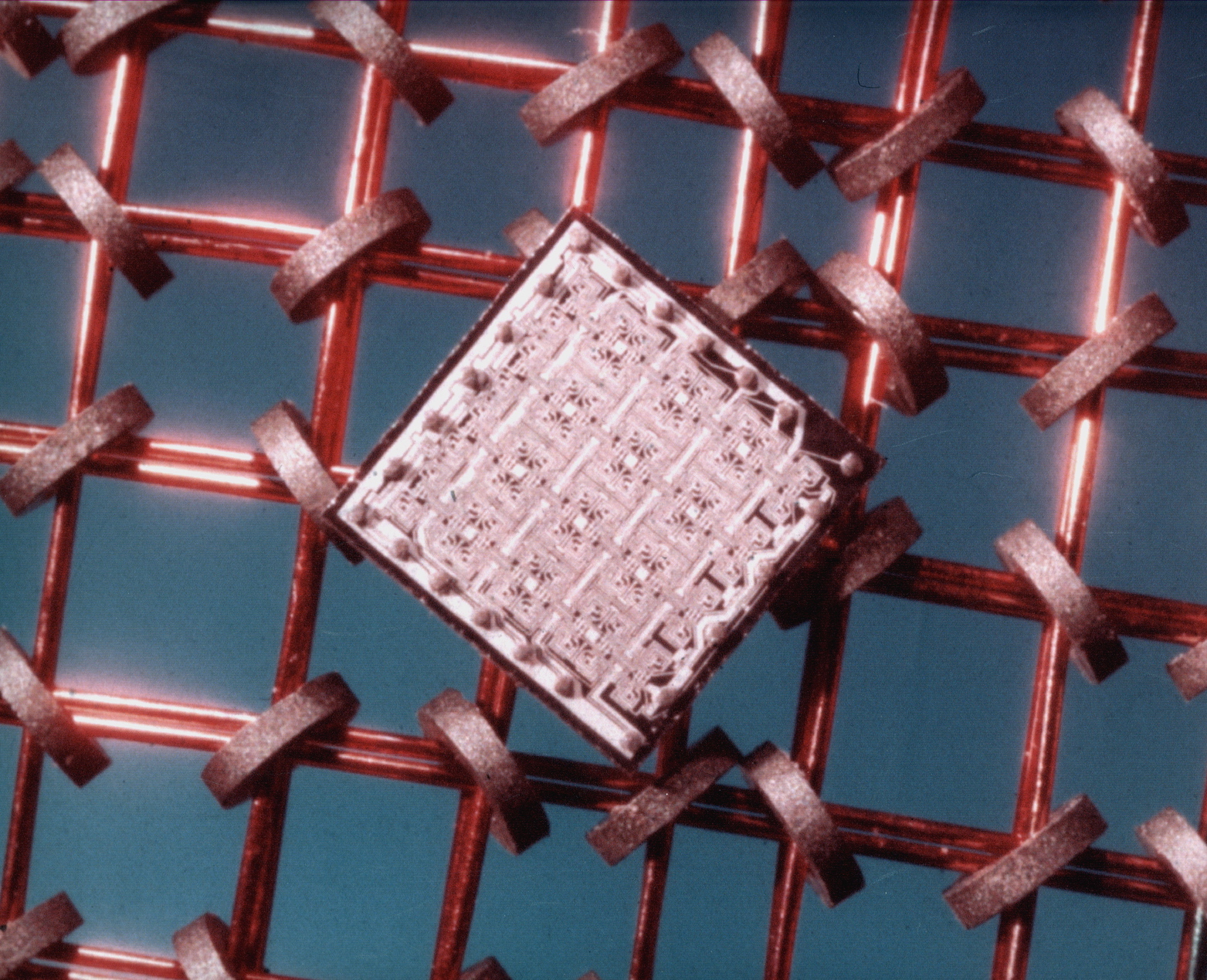
The use of semiconductor RAM dates back to 1965 when IBM introduced the monolithic (single-chip) 16-bit SP95 SRAM chip for their System/360 Model 95 computer, and Toshiba used bipolar DRAM memory cells for its 180-bit Toscal BC-1411 electronic calculator, both based on bipolar transistors. While it offered higher speeds than magnetic-core memory, bipolar DRAM could not compete with the lower price of the then-dominant magnetic-core memory. In 1966, Dr. Robert Dennard invented modern DRAM architecture in which there's a single MOS transistor per capacitor. The first commercial DRAM IC chip, the 1K Intel 1103, was introduced in October 1970. Synchronous dynamic random-access memory (SDRAM) was reintroduced with the Samsung KM48SL2000 chip in 1992.
History

Early computers used relays, mechanical counters or delay lines for main memory functions. Ultrasonic delay lines were serial devices which could only reproduce data in the order it was written. Drum memory could be expanded at relatively low cost but efficient retrieval of memory items requires knowledge of the physical layout of the drum to optimize speed. Latches built out of triode vacuum tubes, and later, out of discrete transistors, were used for smaller and faster memories such as registers. Such registers were relatively large and too costly to use for large amounts of data; generally, only a few dozen or few hundred bits of such memory could be provided.
The first practical form of random-access memory was the Williams tube. It stored data as electrically charged spots on the face of a cathode-ray tube. Since the electron beam of the CRT could read and write the spots on the tube in any order, memory was random access. The capacity of the Williams tube was a few hundred to around a thousand bits, but it was much smaller, faster, and more power-efficient than using individual vacuum tube latches. Developed at the University of Manchester in England, the Williams tube provided the medium on which the first electronically stored program was implemented in the Manchester Baby computer, which first successfully ran a program on 21 June, 1948. In fact, rather than the Williams tube memory being designed for the Baby, the Baby was a testbed to demonstrate the reliability of the memory.
Magnetic-core memory was invented in 1947 and developed up until the mid-1970s. It became a widespread form of random-access memory, relying on an array of magnetized rings. By changing the sense of each ring's magnetization, data could be stored with one bit stored per ring. Since every ring had a combination of address wires to select and read or write it, access to any memory location in any sequence was possible. Magnetic core memory was the standard form of computer memory until displaced by semiconductor memory in integrated circuits (ICs) during the early 1970s.
Prior to the development of integrated read-only memory (ROM) circuits, permanent (or read-only) random-access memory was often constructed using diode matrices driven by address decoders, or specially wound core rope memory planes.
Semiconductor memory appeared in the 1960s with bipolar memory, which used bipolar transistors. Although it was faster, it could not compete with the lower price of magnetic core memory.
MOS RAM
In 1957, Frosch and Derick manufactured the first silicon dioxide field-effect transistors at Bell Labs, the first transistors in which drain and source were adjacent at the surface. Subsequently, in 1960, a team demonstrated a working MOSFET at Bell Labs. This led to the development of metal–oxide–semiconductor (MOS) memory by John Schmidt at Fairchild Semiconductor in 1964. In addition to higher speeds, MOS semiconductor memory was cheaper and consumed less power than magnetic core memory. The development of silicon-gate MOS integrated circuit (MOS IC) technology by Federico Faggin at Fairchild in 1968 enabled the production of MOS memory chips. MOS memory overtook magnetic core memory as the dominant memory technology in the early 1970s.
Integrated bipolar static random-access memory (SRAM) was invented by Robert H. Norman at Fairchild Semiconductor in 1963.{{cite patent
Dynamic random-access memory (DRAM) allowed replacement of a 4- or 6-transistor latch circuit by a single transistor for each memory bit, greatly increasing memory density at the cost of volatility. Data was stored in the tiny capacitance of each transistor and had to be periodically refreshed every few milliseconds before the charge could leak away.
Toshiba's Toscal BC-1411 electronic calculator, which was introduced in 1965, used a form of capacitor bipolar DRAM, storing 180-bit data on discrete memory cells, consisting of germanium bipolar transistors and capacitors. Capacitors had also been used for earlier memory schemes, such as the drum of the Atanasoff–Berry Computer, the Williams tube and the Selectron tube. While it offered higher speeds than magnetic-core memory, bipolar DRAM could not compete with the lower price of the then-dominant magnetic-core memory.

In 1966, Robert Dennard, while examining the characteristics of MOS technology, found it was capable of building capacitors, and that storing a charge or no charge on the MOS capacitor could represent the 1 and 0 of a bit, and the MOS transistor could control writing the charge to the capacitor. This led to his development of modern DRAM architecture for which there is a single MOS transistor per capacitor. In 1967, Dennard filed a patent under IBM for a single-transistor DRAM memory cell, based on MOS technology. The first commercial DRAM IC chip was the Intel 1103, which was manufactured on an 8μm MOS process with a capacity of 1kbit, and was released in 1970.
The earliest DRAMs were often synchronized with the CPU clock and were used with early microprocessors. In the mid-1970s, DRAMs moved to the asynchronous design, but in the 1990s returned to synchronous operation. In 1992 Samsung released KM48SL2000, which had a capacity of 16Mbit. The first commercial double data rate SDRAM was Samsung's 64Mbit DDR SDRAM, released in June 1998. GDDR (graphics DDR) is a form of SGRAM (synchronous graphics RAM), which was first released by Samsung as a 16Mbit memory chip in 1998.
Types
In general, the term RAM refers solely to solid-state memory devices, and more specifically the main memory in most computers. The two widely used forms of modern RAM are static RAM (SRAM) and dynamic RAM (DRAM). In SRAM, a bit of data is stored using the state of a memory cell, typically using six MOSFETs. This form of RAM is more expensive to produce, but is generally faster and requires less static power than DRAM. In modern computers, SRAM is often used as cache memory for the CPU. DRAM stores a bit of data using a transistor and capacitor pair (typically a MOSFET and MOS capacitor, respectively), which together comprise a DRAM cell. The capacitor holds a high or low charge (1 or 0, respectively), and the transistor acts as a switch that lets the control circuitry on the chip read the capacitor's state of charge or change it. As this form of memory is less expensive to produce than static RAM, it is the predominant form of computer memory used in modern computers.
Both static and dynamic RAM are considered volatile, as their state is lost when power is removed from the system. By contrast, read-only memory (ROM) stores data by permanently enabling or disabling selected transistors, such that the memory cannot be altered. Writable variants of ROM (such as EEPROM and NOR flash) share properties of both ROM and RAM, enabling data to persist without power and to be updated without requiring special equipment.
ECC memory (which can be either SRAM or DRAM) includes special circuitry to detect and/or correct random faults (memory errors) in the stored data, using parity bits or error correction codes.
Memory cell
Main article: Memory cell (computing)
The memory cell is the fundamental building block of computer memory. The memory cell is an electronic circuit that stores one bit of binary information. The cell can be set to store a logic 1 (high voltage level) and reset to store a logic 0 (low voltage level). Its value is maintained until it is changed by the set/reset process. The value in the memory cell can be accessed by reading it.
In SRAM, the memory cell is a type of flip-flop circuit, usually implemented using FETs. This means that SRAM requires very low power when not being accessed, but it is complex, expensive and has low storage density.
A second type, DRAM, is based around a capacitor. Charging and discharging this capacitor can store a 1 or a 0 in the cell. However, the charge in this capacitor slowly leaks away and must be refreshed periodically. Because of this refresh process, DRAM uses more power, but it can achieve greater storage densities and lower unit costs compared to SRAM.
| [[File:SRAM Cell (6 Transistors).svg | thumb | class=skin-invert-image | SRAM cell (6 transistors)]] | [[File:DRAM Cell Structure (Model of Single Circuit Cell).PNG | thumb | DRAM cell (1 transistor and one capacitor)]] |
|---|
Addressing
To be useful, memory cells must be readable and writable. Within the RAM device, multiplexing and demultiplexing circuitry is used to select memory cells. Typically, a RAM device has a set of address lines A_0, A_1,...A_n, and for each combination of bits that may be applied to these lines, a set of memory cells are selected. Due to this addressing, RAM devices virtually always have a memory capacity that is a power of two.
Usually, several memory cells share the same address. For example, a 4-bit-wide RAM chip has four memory cells for each address. Often the width of the memory and that of the microprocessor are different; for a 32-bit microprocessor, eight 4-bit RAM chips would be needed.
Often, more addresses are needed than can be provided by a single device. In that case, multiple devices are used, with external multiplexors used to select the device assigned to a specific address range. RAM is often byte addressable, although word-addressable RAM also exists.
Memory hierarchy
Main article: Memory hierarchy
Many computer systems have a memory hierarchy consisting of processor registers, on-die SRAM caches, external caches, DRAM, memory paging systems and virtual memory or swap space on a SSD or hard drive. This entire pool of memory may be referred to as RAM from a programming perspective. The overall goal of using a memory hierarchy is to obtain the fastest possible average access time while minimizing the total cost of the entire memory system.
Other uses of RAM
In addition to serving as temporary storage and working space for the operating system and applications, RAM is used in numerous other ways.
Virtual memory
Main article: Virtual memory
Most modern operating systems employ a method, known as virtual memory, of extending RAM capacity. A portion of the computer's hard drive or SSD is set aside for a paging file or a scratch partition, and the combination of physical RAM and the paging file forms the system's total memory. For example, if a computer has 2 GB of RAM and a 1 GB page file, the operating system has 3 GB total memory available to it. When the system runs low on physical memory, it can swap portions of RAM to the paging file to make room for new data. When the previously swapped information is needed again, another swap is performed to read the information back into RAM. Excessive use of this mechanism results in thrashing and generally hampers overall system performance, mainly because hard drives are far slower than RAM.
RAM disk
Main article: RAM drive
Software can partition a portion of a computer's RAM, allowing it to act as a much faster hard drive that is called a RAM drive. A RAM drive typically loses the stored data when the computer is shut down.
Shadow RAM
Sometimes, the contents of a relatively slow ROM chip are copied to read/write memory to allow for shorter access times. The ROM chip is then disabled while the initialized memory locations are switched in on the same block of addresses (often write-protected). This process, sometimes called shadowing, is fairly common in both computers and embedded systems.
As a common example, the BIOS in typical personal computers often has an option called "use shadow BIOS" or similar. When enabled, functions that rely on data from the BIOS's ROM instead use DRAM locations (most can also toggle shadowing of video card ROM or other ROM sections). Depending on the system, this may not result in increased performance, and may cause incompatibilities. For example, some hardware may be inaccessible to the operating system if shadow RAM is used. On some systems the benefit may be hypothetical because the BIOS is not used after booting in favor of direct hardware access. Free memory is reduced by the size of the shadowed ROMs.
Virtual private networks
Some virtual private network services utilize RAM servers to keep all runtime state including session metadata and cryptographic material in volatile memory so that a power cycle or reboot clears it, reducing persistent forensic artifacts relative to disk-backed designs. In such a design, no data is written to hard drives; all information resides in volatile memory and is erased whenever the server is powered off or rebooted.
Memory wall
The memory wall is the growing disparity of speed between CPU and the response time of memory (known as memory latency) outside the CPU chip. An important reason for this disparity is the limited communication bandwidth beyond chip boundaries. From 1986 to 2000, CPU speed improved at an annual rate of 55% while off-chip memory response time only improved at 10%. Given these trends, it was expected that memory latency would become an overwhelming bottleneck in computer performance.
Another reason for the disparity is the enormous increase in the size of memory since the start of the PC revolution in the 1980s. Originally, PCs contained less than 1 mebibyte of RAM, which often had a response time of 1 CPU clock cycle, meaning that it required 0 wait states. Larger memory units are inherently slower than smaller ones of the same type, simply because it takes longer for signals to traverse a larger circuit. Constructing a memory unit of many gibibytes with a response time of one clock cycle is difficult or impossible. Modern CPUs often still have a mebibyte of 0 wait state cache memory, but it resides on the same chip as the CPU cores due to the bandwidth limitations of chip-to-chip communication. It must also be constructed from static RAM, which is far more expensive than the dynamic RAM used for larger memories. Static RAM also consumes far more power.
CPU speed improvements slowed significantly partly due to major physical barriers and partly because CPU designs have already hit the memory wall in some sense. Intel summarized these causes in a 2005 document.
First of all, as chip geometries shrink and clock frequencies rise, the transistor leakage current increases, leading to excess power consumption and heat... Secondly, the advantages of higher clock speeds are in part negated by memory latency, since memory access times have not been able to keep pace with increasing clock frequencies. Third, for certain applications, traditional serial architectures are becoming less efficient as processors get faster (due to the so-called von Neumann bottleneck), further undercutting any gains that frequency increases might otherwise buy. In addition, partly due to limitations in the means of producing inductance within solid state devices, resistance-capacitance (RC) delays in signal transmission are growing as feature sizes shrink, imposing an additional bottleneck that frequency increases don't address.
The RC delays in signal transmission were also noted in "Clock Rate versus IPC: The End of the Road for Conventional Microarchitectures" which projected a maximum of 12.5% average annual CPU performance improvement between 2000 and 2014.
A different concept is the processor-memory performance gap, which can be addressed by 3D integrated circuits that reduce the distance between the logic and memory aspects that are further apart in a 2D chip. Memory subsystem design requires a focus on the gap, which is widening over time. The main method of bridging the gap is the use of caches; small amounts of high-speed memory that houses recent operations and instructions nearby the processor, speeding up the execution of those operations or instructions in cases where they are called upon frequently. Multiple levels of caching have been developed to deal with the widening gap, and the performance of high-speed modern computers relies on evolving caching techniques. There can be up to a 53% difference between the growth in speed of processor and the lagging speed of main memory access.
Solid-state hard drives have continued to increase in speed, from ~400 Mbit/s via SATA3 in 2012 up to ~7 GB/s via NVMe/PCIe in 2024, closing the gap between RAM and hard disk speeds, although RAM continues to be an order of magnitude faster, with single-lane DDR5 8000MHz capable of 128 GB/s, and modern GDDR even faster. Fast, cheap, non-volatile solid state drives have replaced some functions formerly performed by RAM, such as holding certain data for immediate availability in server farms - 1 terabyte of SSD storage can be had for $200, while 1 TB of RAM would cost thousands of dollars.
Timeline
SRAM
| Date of introduction | Chip name | Capacity (bits) | Access time | SRAM type | Manufacturer(s) | Process | MOSFET | Ref | ||||||||||||
|---|---|---|---|---|---|---|---|---|---|---|---|---|---|---|---|---|---|---|---|---|
| 1 | Bipolar (cell) | Fairchild | ||||||||||||||||||
| 1965 | 8 | Bipolar | IBM | |||||||||||||||||
| SP95 | 16 | Bipolar | IBM | |||||||||||||||||
| 64 | MOSFET | Fairchild | PMOS | last=Sah | first=Chih-Tang | author-link=Chih-Tang Sah | title=Evolution of the MOS transistor-from conception to VLSI | journal=Proceedings of the IEEE | date=October 1988 | volume=76 | issue=10 | pages=1280–1326 (1303) | doi=10.1109/5.16328 | url=http://www.dejazzer.com/ece723/resources/Evolution_of_the_MOS_transistor.pdf | issn=0018-9219 | bibcode=1988IEEEP..76.1280S }} | ||||
| 1966 | TMC3162 | 16 | Bipolar (TTL) | Transitron | ||||||||||||||||
| MOSFET | NEC | |||||||||||||||||||
| 1968 | 64 | MOSFET | Fairchild | PMOS | ||||||||||||||||
| 144 | MOSFET | NEC | NMOS | |||||||||||||||||
| 512 | MOSFET | IBM | NMOS | |||||||||||||||||
| 1969 | 128 | Bipolar | IBM | |||||||||||||||||
| 1101 | 256 | 850 ns | MOSFET | Intel | 12,000 nm | PMOS | title=1970s: SRAM evolution | url=http://www.shmj.or.jp/english/pdf/ic/exhibi724E.pdf | website=Semiconductor History Museum of Japan | access-date=27 June 2019}} | ||||||||||
| 1972 | 2102 | 1 kbit | MOSFET | Intel | NMOS | |||||||||||||||
| 1974 | 5101 | 1 kbit | 800 ns | MOSFET | Intel | CMOS | title=Component Data Catalog | date=1978 | publisher=Intel | page=3 | url=http://bitsavers.trailing-edge.com/components/intel/_dataBooks/1978_Intel_Component_Data_Catalog.pdf | access-date=27 June 2019}} | ||||||||
| 2102A | 1 kbit | 350 ns | MOSFET | Intel | NMOS (depletion) | title=Silicon Gate MOS 2102A | url=https://drive.google.com/file/d/0B9rh9tVI0J5mMmZlYWRlMDQtNDYzYS00OWJkLTg4YzYtZDYzMzc5Y2ZlYmVk/view | publisher=Intel | access-date=27 June 2019}} | |||||||||||
| 1975 | 2114 | 4 kbit | 450 ns | MOSFET | Intel | NMOS | ||||||||||||||
| 1976 | 2115 | 1 kbit | 70 ns | MOSFET | Intel | NMOS (HMOS) | ||||||||||||||
| 2147 | 4 kbit | 55 ns | MOSFET | Intel | NMOS (HMOS) | title=1978: Double-well fast CMOS SRAM (Hitachi) | url=http://www.shmj.or.jp/english/pdf/ic/exhibi727E.pdf | website=Semiconductor History Museum of Japan | access-date=5 July 2019}} | |||||||||||
| 1977 | 4 kbit | MOSFET | Toshiba | CMOS | ||||||||||||||||
| 1978 | HM6147 | 4 kbit | 55 ns | MOSFET | Hitachi | 3,000 nm | CMOS (twin-well) | |||||||||||||
| TMS4016 | 16 kbit | MOSFET | Texas Instruments | NMOS | ||||||||||||||||
| 1980 | 16 kbit | MOSFET | Hitachi, Toshiba | CMOS | ||||||||||||||||
| 64 kbit | MOSFET | Matsushita | ||||||||||||||||||
| 1981 | 16 kbit | MOSFET | Texas Instruments | 2,500 nm | NMOS | |||||||||||||||
| 4 kbit | 18 ns | MOSFET | Matsushita, Toshiba | 2,000 nm | CMOS | |||||||||||||||
| 1982 | 64 kbit | MOSFET | Intel | 1,500 nm | NMOS (HMOS) | |||||||||||||||
| 64 kbit | 50 ns | MOSFET | Mitsubishi | CMOS | ||||||||||||||||
| 1984 | 256 kbit | MOSFET | Toshiba | 1,200 nm | CMOS | |||||||||||||||
| 1987 | 1 Mbit | MOSFET | Sony, Hitachi, Mitsubishi, Toshiba | CMOS | ||||||||||||||||
| 256 kbit | 10 ns | BiMOS | Texas Instruments | 800 nm | BiCMOS | |||||||||||||||
| 1990 | 4 Mbit | 1523 ns | MOSFET | NEC, Toshiba, Hitachi, Mitsubishi | CMOS | |||||||||||||||
| 1992 | 16 Mbit | 1215 ns | MOSFET | Fujitsu, NEC | 400 nm | |||||||||||||||
| 512 kbit | 2.5 ns | MOSFET | IBM | CMOS (SOI) | ||||||||||||||||
| 1995 | 4 Mbit | 6 ns | Cache (SyncBurst) | Hitachi | 100 nm | CMOS | ||||||||||||||
| 256 Mbit | MOSFET | Hyundai | CMOS | title=History: 1990s | url=https://www.skhynix.com/eng/about/history1990.jsp | website=SK Hynix | access-date=6 July 2019 | archive-date=5 February 2021 | archive-url=https://web.archive.org/web/20210205032928/https://www.skhynix.com/eng/about/history1990.jsp | url-status=dead }} |
DRAM
| Date of introduction | Chip name | Capacity (bits) | DRAM type | Manufacturer(s) | Process | MOSFET | Area | Ref | ||||||||||
|---|---|---|---|---|---|---|---|---|---|---|---|---|---|---|---|---|---|---|
| 1965 | 1 bit | DRAM (cell) | Toshiba | url=http://www.oldcalculatormuseum.com/s-toshbc1411.html | title=Spec Sheet for Toshiba "TOSCAL" BC-1411 | website=Old Calculator Web Museum | access-date=8 May 2018 | url-status=live | archive-url=https://web.archive.org/web/20170703071307/http://www.oldcalculatormuseum.com/s-toshbc1411.html | archive-date=3 July 2017}} | ||||||||
| 1967 | 1 bit | DRAM (cell) | IBM | MOS | title=Robert Dennard | url=https://www.britannica.com/biography/Robert-Dennard | website=Encyclopedia Britannica | access-date=8 July 2019}} | ||||||||||
| 1968 | 256 bit | DRAM (IC) | Fairchild | PMOS | title=1970: Semiconductors compete with magnetic cores | url=https://www.computerhistory.org/storageengine/semiconductors-compete-with-magnetic-cores/ | website=Computer History Museum | access-date=19 June 2019}} | ||||||||||
| 1969 | 1 bit | DRAM (cell) | Intel | PMOS | ||||||||||||||
| 1970 | 1102 | 1 kbit | DRAM (IC) | Intel, Honeywell | PMOS | |||||||||||||
| 1103 | 1 kbit | DRAM | Intel | 8,000 nm | PMOS | 10 mm2 | title=Intel: 35 Years of Innovation (1968–2003) | url=https://www.intel.com/Assets/PDF/General/35yrs.pdf | publisher=Intel | year=2003 | access-date=26 June 2019}} | |||||||
| 1971 | μPD403 | 1 kbit | DRAM | NEC | NMOS | |||||||||||||
| 2 kbit | DRAM | General Instrument | PMOS | 13 mm2 | last1=Gealow | first1=Jeffrey Carl | title=Impact of Processing Technology on DRAM Sense Amplifier Design | url=https://core.ac.uk/download/pdf/4426308.pdf | publisher=Massachusetts Institute of Technology | via=CORE | date=10 August 1990 | pages=149–166 | access-date=25 June 2019}} | |||||
| 1972 | 2107 | 4 kbit | DRAM | Intel | NMOS | url=http://download.intel.com/museum/research/arc_collect/timeline/TimelineDateSort7_05.pdf | title=A chronological list of Intel products. The products are sorted by date. | date=July 2005 | work=Intel museum | publisher=Intel Corporation | archive-url=https://web.archive.org/web/20070809053720/http://download.intel.com/museum/research/arc_collect/timeline/TimelineDateSort7_05.pdf | archive-date=August 9, 2007 | access-date=July 31, 2007}} | |||||
| 1973 | 8 kbit | DRAM | IBM | PMOS | 19 mm2 | |||||||||||||
| 1975 | 2116 | 16 kbit | DRAM | Intel | NMOS | |||||||||||||
| 1977 | 64 kbit | DRAM | NTT | NMOS | 35 mm2 | |||||||||||||
| 1979 | MK4816 | 16 kbit | PSRAM | Mostek | NMOS | |||||||||||||
| 64 kbit | DRAM | Siemens | VMOS | 25 mm2 | ||||||||||||||
| 1980 | 256 kbit | DRAM | NEC, NTT | 1,0001,500 nm | NMOS | 3442 mm2 | ||||||||||||
| 1981 | 288 kbit | DRAM | IBM | MOS | 25 mm2 | |||||||||||||
| 1983 | 64 kbit | DRAM | Intel | 1,500 nm | CMOS | 20 mm2 | ||||||||||||
| 256 kbit | DRAM | NTT | CMOS | 31 mm2 | ||||||||||||||
| 8 Mbit | DRAM | Hitachi | MOS | |||||||||||||||
| 1 Mbit | DRAM | Hitachi, NEC | 1,000 nm | NMOS | 7476 mm2 | last1=Robinson | first1=Arthur L. | title=Experimental Memory Chips Reach 1 Megabit: As they become larger, memories become an increasingly important part of the integrated circuit business, technologically and economically | journal=Science | date=11 May 1984 | volume=224 | issue=4649 | pages=590–592 | doi=10.1126/science.224.4649.590 | pmid=17838349 | issn=0036-8075}} | ||
| NTT | 800 nm | CMOS | 53 mm2 | |||||||||||||||
| 1984 | TMS4161 | 64 kbit | DPRAM (VRAM) | Texas Instruments | NMOS | title=MOS Memory Data Book | url=http://bitsavers.trailing-edge.com/components/ti/_dataBooks/1984_TI_MOS_Memory_Data_Book.pdf | publisher=Texas Instruments | year=1984 | pages=4–15 | access-date=21 June 2019}} | |||||||
| μPD41264 | 256 kbit | DPRAM (VRAM) | NEC | NMOS | ||||||||||||||
| 1 Mbit | PSRAM | Toshiba | CMOS | |||||||||||||||
| 1986 | 4 Mbit | DRAM | NEC | 800 nm | NMOS | 99 mm2 | ||||||||||||
| Texas Instruments, Toshiba | 1,000 nm | CMOS | 100137 mm2 | |||||||||||||||
| 1987 | 16 Mbit | DRAM | NTT | 700 nm | CMOS | 148 mm2 | ||||||||||||
| 512 kbit | HSDRAM | IBM | 1,000 nm | CMOS | 78 mm2 | |||||||||||||
| 1991 | 64 Mbit | DRAM | Matsushita, Mitsubishi, Fujitsu, Toshiba | 400 nm | CMOS | |||||||||||||
| 1993 | 256 Mbit | DRAM | Hitachi, NEC | 250 nm | CMOS | |||||||||||||
| 1995 | 4 Mbit | DPRAM (VRAM) | Hitachi | CMOS | title=Japanese Company Profiles | url=http://smithsonianchips.si.edu/ice/cd/PROF96/JAPAN.PDF | publisher=Smithsonian Institution | year=1996 | access-date=27 June 2019}} | |||||||||
| 1 Gbit | DRAM | NEC | 250 nm | CMOS | ||||||||||||||
| Hitachi | 160 nm | CMOS | ||||||||||||||||
| 1996 | 4 Mbit | FRAM | Samsung | NMOS | ||||||||||||||
| 1997 | 4 Gbit | QLC | NEC | 150 nm | CMOS | |||||||||||||
| 1998 | 4 Gbit | DRAM | Hyundai | CMOS | ||||||||||||||
| 4 Gbit | DRAM | Samsung | 100 nm | CMOS | title=A Study of the DRAM industry | url=https://dspace.mit.edu/bitstream/handle/1721.1/59138/659514510-MIT.pdf | publisher=MIT | date=8 June 2010 | access-date=29 June 2019}} | |||||||||
| TC51W3216XB | 32 Mbit | PSRAM | Toshiba | CMOS |
SDRAM
Notes
References
References
- "RAM".
- "RAM".
- Gallagher, Sean. (April 4, 2013). "Memory that never forgets: non-volatile DIMMs hit the market".
- "1966: Semiconductor RAMs Serve High-speed Storage Needs".
- "Field-effect transistor memory".
- "IBM Archives -- FAQ's for Products and Services". ibm.com.
- Napper, Brian. "Computer 50: The University of Manchester Celebrates the Birth of the Modern Computer".
- (Sep 1948). "Electronic Digital Computers". Nature.
- (Feb 1951). "Universal High-Speed Digital Computers: A Small-Scale Experimental Machine". Proc. IEE.
- (1957). "Surface Protection and Selective Masking during Diffusion in Silicon". Journal of the Electrochemical Society.
- KAHNG, D.. (1991). "Silicon-Silicon Dioxide Surface Device". Technical Memorandum of Bell Laboratories.
- Lojek, Bo. (2007). "History of Semiconductor Engineering". Springer-Verlag Berlin Heidelberg.
- (1965). "Solid State Design – Vol. 6". Horizon House.
- "1968: Silicon Gate Technology Developed for ICs".
- (9 August 2017). "DRAM". [[IBM]].
- [http://collection.sciencemuseum.org.uk/objects/co8406093/toscal-bc-1411-calculator-with-electronic-calculator Toscal BC-1411 calculator]. {{webarchive. link. (2017-07-29, [[Science Museum, London]].)
- "1966: Semiconductor RAMs Serve High-speed Storage Needs".
- Bellis, Mary. "Who Invented the Intel 1103 DRAM Chip?".
- P. Darche. (2020). "Microprocessor: Prolegomenes - Calculation and Storage Functions - Calculation Models and Computer". John Wiley & Sons.
- (2008). "Memory Systems: Cache, DRAM, Disk". Morgan Kaufmann.
- (1993). "Electronic Design". Hayden Publishing Company.
- (August 1992). "KM48SL2000-7 Datasheet". [[Samsung]].
- (10 February 1999). "Samsung Electronics Develops First 128Mb SDRAM with DDR/SDR Manufacturing Option". [[Samsung]].
- (17 September 1998). "Samsung Electronics Comes Out with Super-Fast 16M DDR SGRAMs". [[Samsung]].
- (2002). "Semiconductor Devices: Physics and Technology". [[Wiley (publisher).
- (2006). "The Essentials of Computer Organization and Architecture". Jones & Bartlett Learning.
- (25 October 2020). "Foundations of Computer Technology". CRC Press.
- "Shadow Ram".
- (2022-07-20). "The Evolution of Volatile Memory Forensics". Journal of Cybersecurity and Privacy.
- (2020). "Performance Analysis of VPN Gateways".
- Castro, Chiara. (2022-05-20). "ExpressVPN TrustedServer - everything you need to know".
- "Archived copy".
- (March 2, 2005). "Platform 2015: Intel Processor and Platform Evolution for the Next Decade".
- (June 10–14, 2000). "Clock Rate versus IPC: The End of the Road for Conventional Microarchitectures".
- Rainer Waser. (2012). "Nanoelectronics and Information Technology". John Wiley & Sons.
- Chris Jesshope and Colin Egan. (2006). "Advances in Computer Systems Architecture: 11th Asia-Pacific Conference, ACSAC 2006, Shanghai, China, September 6-8, 2006, Proceedings". Springer.
- Ahmed Amine Jerraya and Wayne Wolf. (2005). "Multiprocessor Systems-on-chips". Morgan Kaufmann.
- Celso C. Ribeiro and Simone L. Martins. (2004). "Experimental and Efficient Algorithms: Third International Workshop, WEA 2004, Angra Dos Reis, Brazil, May 25-28, 2004, Proceedings, Volume 3". Springer.
- (2018-09-03). "SSD Prices Continue to Fall, Now Upgrade Your Hard Drive!".
- Coppock, Mark. (31 January 2017). "If you're buying or upgrading your PC, expect to pay more for RAM".
- "1966: Semiconductor RAMs Serve High-speed Storage Needs".
- (1965). "IBM first in IC memory". IBM Corporation.
- Sah, Chih-Tang. (October 1988). "Evolution of the MOS transistor-from conception to VLSI". [[Proceedings of the IEEE]].
- "1970s: SRAM evolution".
- (2012). "Advanced CMOS Process Technology". [[Elsevier]].
- "Intel Memory".
- (1978). "Component Data Catalog". [[Intel]].
- "Silicon Gate MOS 2102A". [[Intel]].
- "1978: Double-well fast CMOS SRAM (Hitachi)".
- (October 1981). "An 18 ns CMOS/SOS 4K static RAM". [[IEEE Journal of Solid-State Circuits]].
- (1983). "1983 IEEE International Solid-State Circuits Conference. Digest of Technical Papers".
- (December 1987). "1987 International Electron Devices Meeting".
- (December 1994). "A room temperature 0.1 μm CMOS on SOI". [[IEEE Transactions on Electron Devices]].
- "History: 1990s".
- "Spec Sheet for Toshiba "TOSCAL" BC-1411".
- [http://www.oldcalculatormuseum.com/toshbc1411.html Toshiba "Toscal" BC-1411 Desktop Calculator] {{webarchive. link. (2007-05-20)
- "Robert Dennard".
- (2019-01-23). "Late 1960s: Beginnings of MOS memory".
- "1970: Semiconductors compete with magnetic cores".
- (2003). "Intel: 35 Years of Innovation (1968–2003)". Intel.
- [http://history-computer.com/ModernComputer/Basis/dram.html ''The DRAM memory of Robert Dennard''] {{Webarchive. link. (2020-08-01 history-computer.com)
- (2007). "History of Semiconductor Engineering". [[Springer Science & Business Media]].
- "Manufacturers in Japan enter the DRAM market and integration densities are improved".
- (10 August 1990). "Impact of Processing Technology on DRAM Sense Amplifier Design". [[Massachusetts Institute of Technology]].
- (July 2005). "A chronological list of Intel products. The products are sorted by date.". Intel Corporation.
- "Silicon Gate MOS 2107A". [[Intel]].
- "One of the Most Successful 16K Dynamic RAMs: The 4116". [[Smithsonian Institution]].
- (March 1979). "Memory Data Book And Designers Guide". [[Mostek]].
- "The Cutting Edge of IC Technology: The First 294,912-Bit (288K) Dynamic RAM". [[Smithsonian Institution]].
- "Computer History for 1984".
- (1987). "Japanese Technical Abstracts". University Microfilms.
- (11 May 1984). "Experimental Memory Chips Reach 1 Megabit: As they become larger, memories become an increasingly important part of the integrated circuit business, technologically and economically". [[Science (journal).
- (1984). "MOS Memory Data Book". [[Texas Instruments]].
- (10 January 2019). "Famous Graphics Chips: TI TMS34010 and VRAM".
- "μPD41264 256K Dual Port Graphics Buffer". [[NEC Electronics]].
- "Sense amplifier circuit for switching plural inputs at low power".
- (1987). "Fine CMOS techniques create 1M VSRAM". University Microfilms.
- (October 1988). "A 20-ns 128-kbit*4 high speed DRAM with 330-Mbit/s data rate". [[IEEE Journal of Solid-State Circuits]].
- "Memory".
- (1996). "Japanese Company Profiles". [[Smithsonian Institution]].
- {{usurped
- (2003). "Nanostructures: Synthesis, Functional Properties and Application". [[Springer Science & Business Media]].
- (8 June 2010). "A Study of the DRAM industry". [[MIT]].
- (24 June 2001). "Toshiba's new 32 Mb Pseudo-SRAM is no fake". The Engineer.
This article was imported from Wikipedia and is available under the Creative Commons Attribution-ShareAlike 4.0 License. Content has been adapted to SurfDoc format. Original contributors can be found on the article history page.
Ask Mako anything about Random-access memory — get instant answers, deeper analysis, and related topics.
Research with MakoFree with your Surf account
Create a free account to save articles, ask Mako questions, and organize your research.
Sign up freeThis content may have been generated or modified by AI. CloudSurf Software LLC is not responsible for the accuracy, completeness, or reliability of AI-generated content. Always verify important information from primary sources.
Report