From Surf Wiki (app.surf) — the open knowledge base
Radeon HD 4000 series
Series of video cards

Series of video cards
| Field | Value | |
|---|---|---|
| name | ATI Radeon HD 4000 series | |
| image | [[Image:ATI Radeon Graphics Logo.svg | ATI Radeon logo]] |
| codename | Radeon R700 series | |
| M9x series | ||
| created | ||
| transistors1 | 242M 55 nm (RV710) | |
| transistors2 | 514M 55 nm (RV730) | |
| transistors3 | 826M 40 nm (RV740) | |
| transistors5 | 956M 55 nm (RV770) | |
| transistors6 | 959M 55 nm (RV790) | |
| architecture | TeraScale 1 | |
| entry | 4350, 4550, 4570 | |
| midrange | 4650, 4670, 4730, 4750, 4770 | |
| highend | 4830, 4850, 4860, 4870 | |
| enthusiast | 4890, 4850X2, 4870X2 | |
| openglversion | OpenGL 3.3 | |
| d3dversion | Direct3D 10.1 | |
| Shader Model 4.1 | ||
| openclversion | OpenCL 1.1 | |
| predecessor | Radeon HD 3000 series | |
| successor | Radeon HD 5000 series | |
| support status | Unsupported |
M9x series Shader Model 4.1
The Radeon R700 is the engineering codename for a graphics processing unit series developed by Advanced Micro Devices under the ATI brand name. The foundation chip, codenamed RV770, was announced and demonstrated on June 16, 2008 as part of the FireStream 9250 and Cinema 2.0 initiative launch media event, with official release of the Radeon HD 4800 series on June 25, 2008. Other variants include enthusiast-oriented RV790, mainstream product RV730, RV740 and entry-level RV710.
Its direct competition was NVIDIA's GeForce 200 series, which launched in the same month.
Architecture
This article is about all products under the brand "Radeon HD 4000 Series". All products implement TeraScale 1 microarchitecture.
Execution units
The RV770 extends the R600's unified shader architecture by increasing the stream processing unit count to 800 units (up from 320 units in the R600), which are grouped into 10 SIMD cores composed of 16 shader cores containing 4 FP MADD/DP ALUs and 1 MADD/transcendental ALU. The RV770 retains the R600's 4 Quad ROP cluster count, however, they are faster and now have dedicated hardware-based AA resolve in addition to the shader-based resolve of the R600 architecture. The RV770 also has 10 texture units, each of which can handle 4 addresses, 16 FP32 samples, and 4 FP32 filtering functions per clock cycle.
Memory and internal buses
RV770 features a 256-bit memory controller and is the first GPU to support GDDR5 memory, which runs at 900 MHz giving an effective transfer rate of 3.6 GHz and memory bandwidth of up to 115 GB/s. The internal ring bus from the R520 and R600 has been replaced by the combination of a crossbar and an internal hub.
Video acceleration
The SIP block UVD 2.0-2.2 implemented on the dies of all Radeon HD 4000 Series Desktop gpus, 48xx series is using uvd 2.0, 47xx-46xx-45xx-43xx series is using uvd 2.2.
Support is available for Microsoft Windows at release, for Linux with Catalyst 8.10. The free and open-source driver requires Linux kernel 3.10 in combination with Mesa 9.1 (exposed via the widely adopted VDPAU)), offering full hardware MPEG-2, H.264/MPEG-4 AVC and VC-1 decoding and the support for dual video streams, the Advanced Video Processor (AVP) also saw an upgrade with DVD upscaling capability and dynamic contrast feature. The RV770 series GPU also supports xvYCC color space output and 7.1 surround sound output (LPCM, AC3, DTS) over HDMI. The RV770 GPU also supports an Accelerated Video Transcoding (AVT) feature, which has video transcoding functions being assisted by the GPU, through stream processing.
GPU interconnect enhancements
This generation of dual-GPU design retains the use of a PCI Express bridge, PLX PEX 8647 with a power dissipation of 3.8 watts inclusive of PCI Express 2.0 support, allowing two GPUs on the same PCI Express slot with doubled bandwidth over the past generation of product (Radeon HD 3870 X2). Subsequent generations of dual-GPU design also feature an interconnect for inter-GPU communications through the implementation of a CrossFire X SidePort on each GPU, giving extra 5 GB/s full-duplex inter-GPU bandwidth. These two features increase total bandwidth for dual-GPU designs to 21.8 GB/s.
OpenCL (API)
OpenCL accelerates many scientific Software Packages against CPU up to factor 10 or 100 and more. Open CL 1.0 to 1.1 are supported for all Chips with RV7xx.
Desktop products
Main article: List of AMD graphics processing units#Radeon HD 4000 Series
Radeon HD 4800
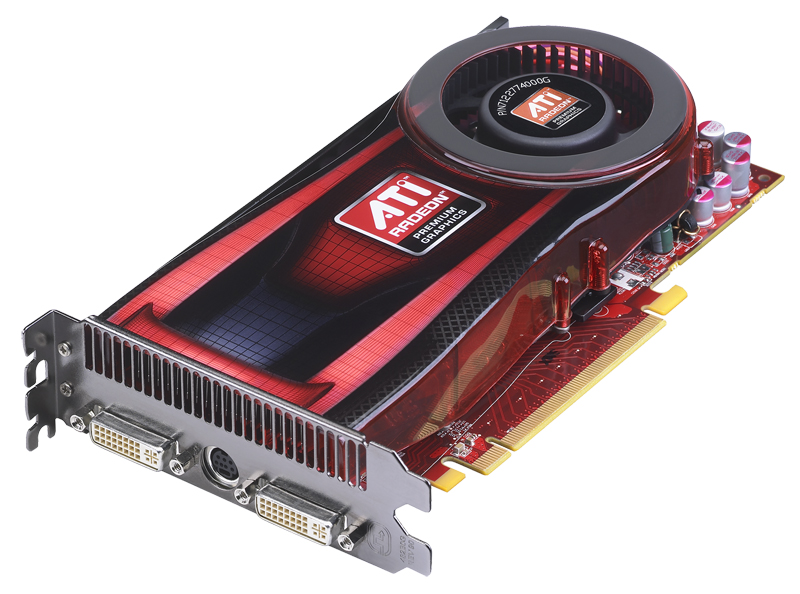
The Radeon HD 4850 was announced on June 19, 2008 while the Radeon HD 4870 was announced on June 25, 2008. They are both based on the RV770 GPU, packing 956 million transistors and being produced on a 55 nm process. The Radeon HD 4850 currently uses GDDR3 memory, while the Radeon HD 4870 uses GDDR5 memory.
Another variant, the Radeon HD 4830 was updated on October 23, 2008, featuring the RV770 LE GPU with a 256-bit GDDR3 memory interface, and 640 shader processors. Basically the RV770 LE is a RV770 with some functional units disabled.
Dual GPU products using two RV770 GPUs, codenamed R700, were also announced. One product named Radeon HD 4870 X2, featuring 2×1GB GDDR5 memory, was released on August 12, 2008, while another dual-GPU product, the Radeon HD 4850 X2, with GDDR3 memory and lower clock speeds, is also available.
A minor update was introduced on April 2, 2009 with the launch of Radeon HD 4890 graphics cards based on the RV790 GPU. Featuring an improved design with decoupling capacitors to reduce signal noise, altered ASIC power distribution and re-timed the whole GPU chip, which resulted in a slight increase in die size but overall much better stability at high clock rates and a higher default clock. On August 18, 2009, AMD released a stripped down variant of the RV790 GPU called the RV790GT that is used by the Radeon HD 4860 which is now available in all markets.
Radeon HD 4700
The Radeon HD 4700 series was announced on April 28, 2009. The Radeon HD 4770, is based on the RV740 GPU, packs 826 million transistors and being produced on the latest 40 nm process. The Radeon HD 4730 was introduced June 8, 2009, unlike the RV740 based Radeon HD 4770, the 4730 is a stripped down 55 nm RV770 GPU, named the RV770CE. The 4730 packs 956 million transistors, and uses GDDR5 memory on a 128-bit bus. On September 9, 2009, the RV740PRO based Radeon HD 4750 was released exclusively to the Chinese market. The Radeon HD 4750 is based on the 40 nm RV740 of the Radeon HD 4770 but features a lower clock speed and the absence of a six-pin auxiliary power input.
Radeon HD 4600
The Radeon HD 4600 series was announced on September 10, 2008. All variants are based on the RV730 GPU, packing 514 million transistors and being produced on a 55 nm process. The PCIe version 4600 series products do not require external power connectors. More recently, an AGP version of the 4670 has been released. This does require an external power connector. As of March 2018, this elusive AGP card remains among the last cards using the aging bus.
Radeon HD 4300/HD 4500

The Radeon HD 4350 and Radeon HD 4550 were announced on September 30, 2008, both based on the RV710 GPU, packing 242 million transistors and being produced on a 55 nm process. Both products use either GDDR3, DDR3 or DDR2 video memory. AMD states these two products have maximum of 20 W and 25 W of power consumption under full load, respectively.
Chipset Table
Main article: List of AMD graphics processing units#Radeon HD 4000 series, TeraScale (microarchitecture)#TeraScale 1
Desktop Products
| Model4 | Launch | Code name | Fab (nm) | Transistors (million) | Die size (mm2) | Bus interface | Clock rate | Core config1 | Fillrate | Memory2 | Processing power | |||||||||||||||||||||||||||||||||||||||||||||||||||||||||||||||||||
|---|---|---|---|---|---|---|---|---|---|---|---|---|---|---|---|---|---|---|---|---|---|---|---|---|---|---|---|---|---|---|---|---|---|---|---|---|---|---|---|---|---|---|---|---|---|---|---|---|---|---|---|---|---|---|---|---|---|---|---|---|---|---|---|---|---|---|---|---|---|---|---|---|---|---|---|---|---|---|
| (GFLOPS) | TDP3 (Watts) | Crossfire support | API support (version) | Release Price (USD) | Core (MHz) | Memory (MHz) | Pixel (GP/s) | Texture (GT/s) | Size (MB) | Bandwidth (GB/s) | Bus type | Bus width (bit) | Single precision | Double precision | Idle | Max. | Direct3D | OpenGL | OpenCL | Radeon HD 4350 | Radeon HD 4550 | Radeon HD 4570 | Radeon HD 4580 | Radeon HD 4650 | Radeon HD 4670 | Radeon HD 4730 | Radeon HD 4750 | Radeon HD 4770 | Radeon HD 4810 | Radeon HD 4830 | Radeon HD 4850 | Radeon HD 4860 | Radeon HD 4870 | Radeon HD 4890 | Radeon HD 4850 X2 | Radeon HD 4870 X2 | Model4 | Launch | Code name | Fab (nm) | Transistors (million) | Die size (mm2) | Bus interface | Clock rate | Core config1 | Fillrate | Memory2 | Processing power | ||||||||||||||||||||||||||||||
| (GFLOPS) | TDP3 (Watts) | Crossfire Support | API support (version) | Release Price (USD) | Core (MHz) | Memory (MHz) | Pixel (GP/s) | Texture (GT/s) | Size (MB) | Bandwidth (GB/s) | Bus type | Bus width (bit) | Single precision | Double precision | Idle | Max. | Direct3D | OpenGL | OpenCL | |||||||||||||||||||||||||||||||||||||||||||||||||||||||||||
| Sep 30, 2008 | RV710 | 55 | 242 | 73 | PCIe 2.0 ×16 | |||||||||||||||||||||||||||||||||||||||||||||||||||||||||||||||||||||||||
| PCIe 2.0 ×1 | ||||||||||||||||||||||||||||||||||||||||||||||||||||||||||||||||||||||||||||||
| AGP 8× | 600 | 400 | ||||||||||||||||||||||||||||||||||||||||||||||||||||||||||||||||||||||||||||
| 650 | 80:8:4 | 2.40 | 4.80 | 256 | ||||||||||||||||||||||||||||||||||||||||||||||||||||||||||||||||||||||||||
| 512 | ||||||||||||||||||||||||||||||||||||||||||||||||||||||||||||||||||||||||||||||
| 1024 | 6.40 | |||||||||||||||||||||||||||||||||||||||||||||||||||||||||||||||||||||||||||||
| 10.4 | DDR2 | |||||||||||||||||||||||||||||||||||||||||||||||||||||||||||||||||||||||||||||
| DDR3 | 64 | 92.0 | 20 | rowspan="4" | 10.1 | 3.3 | 1.0 | ? | ||||||||||||||||||||||||||||||||||||||||||||||||||||||||||||||||||||||
| Sep 30, 2008 | RV710 | 55 | 242 | 73 | PCIe 2.0 ×16 | 600 | ||||||||||||||||||||||||||||||||||||||||||||||||||||||||||||||||||||||||
| 600 | 655 | |||||||||||||||||||||||||||||||||||||||||||||||||||||||||||||||||||||||||||||
| 800 | 80:8:4 | 2.40 | 4.80 | 256 | ||||||||||||||||||||||||||||||||||||||||||||||||||||||||||||||||||||||||||
| 512 | ||||||||||||||||||||||||||||||||||||||||||||||||||||||||||||||||||||||||||||||
| 1024 | 10.5 | |||||||||||||||||||||||||||||||||||||||||||||||||||||||||||||||||||||||||||||
| 12.8 | DDR2 | |||||||||||||||||||||||||||||||||||||||||||||||||||||||||||||||||||||||||||||
| GDDR3 | 64 | 96.0 | 25 | 10.1 | 3.3 | 1.0 | ? | |||||||||||||||||||||||||||||||||||||||||||||||||||||||||||||||||||||||
| Nov 25, 2008 | RV710 | 55 | 242 | 73 | PCIe 2.0 ×16 | 650 | 500 | 80:8:4 | 2.60 | 5.20 | 1024 | 8.00 | DDR2 | 64 | 104.0 | 25 | 10.1 | 3.3 | 1.0 | ? | ||||||||||||||||||||||||||||||||||||||||||||||||||||||||||
| Nov 20, 2011 | RV635 PRO | 55 | 378 | 135 | PCIe 2.0 ×16 | 796 | 693 | 120:8:4 | 3.18 | 6.37 | 512 | 22.2 | GDDR3 | 128 | 191.0 | 65 | 10.1 | 3.3 | 1.0 | ? | ||||||||||||||||||||||||||||||||||||||||||||||||||||||||||
| Sep 10, 2008 | RV730 PRO | 55 | 514 | 146 | PCIe 2.0 ×16 | |||||||||||||||||||||||||||||||||||||||||||||||||||||||||||||||||||||||||
| AGP 8× | 600 | |||||||||||||||||||||||||||||||||||||||||||||||||||||||||||||||||||||||||||||
| 650 | 400 - 500 | |||||||||||||||||||||||||||||||||||||||||||||||||||||||||||||||||||||||||||||
| 500 | ||||||||||||||||||||||||||||||||||||||||||||||||||||||||||||||||||||||||||||||
| 700 | 320:32:8 | 4.80 | ||||||||||||||||||||||||||||||||||||||||||||||||||||||||||||||||||||||||||||
| 5.20 | 19.2 | |||||||||||||||||||||||||||||||||||||||||||||||||||||||||||||||||||||||||||||
| 20.8 | 256 | |||||||||||||||||||||||||||||||||||||||||||||||||||||||||||||||||||||||||||||
| 512 | ||||||||||||||||||||||||||||||||||||||||||||||||||||||||||||||||||||||||||||||
| 1024 | 12.8 - 16.0 | |||||||||||||||||||||||||||||||||||||||||||||||||||||||||||||||||||||||||||||
| 16.0 | ||||||||||||||||||||||||||||||||||||||||||||||||||||||||||||||||||||||||||||||
| 22.4 | DDR2 | |||||||||||||||||||||||||||||||||||||||||||||||||||||||||||||||||||||||||||||
| GDDR3 | ||||||||||||||||||||||||||||||||||||||||||||||||||||||||||||||||||||||||||||||
| GDDR4 | 64 | |||||||||||||||||||||||||||||||||||||||||||||||||||||||||||||||||||||||||||||
| 128 | 384.0 | |||||||||||||||||||||||||||||||||||||||||||||||||||||||||||||||||||||||||||||
| 416.0 | 48 | 2-Way Crossfire | 10.1 | 3.3 | 1.0 | ? | ||||||||||||||||||||||||||||||||||||||||||||||||||||||||||||||||||||||||
| Sep 10, 2008 | RV730 XT | 55 | 514 | 146 | PCIe 2.0 ×16 | |||||||||||||||||||||||||||||||||||||||||||||||||||||||||||||||||||||||||
| AGP 8× | 750 | |||||||||||||||||||||||||||||||||||||||||||||||||||||||||||||||||||||||||||||
| 750 | 400 - 500 | |||||||||||||||||||||||||||||||||||||||||||||||||||||||||||||||||||||||||||||
| 900 | ||||||||||||||||||||||||||||||||||||||||||||||||||||||||||||||||||||||||||||||
| 1000 | 320:32:8 | 6.00 | 24.0 | 512 | ||||||||||||||||||||||||||||||||||||||||||||||||||||||||||||||||||||||||||
| 1024 | 12.8 - 16.0 | |||||||||||||||||||||||||||||||||||||||||||||||||||||||||||||||||||||||||||||
| 28.8 | ||||||||||||||||||||||||||||||||||||||||||||||||||||||||||||||||||||||||||||||
| 32.0 | DDR2 | |||||||||||||||||||||||||||||||||||||||||||||||||||||||||||||||||||||||||||||
| GDDR3 | ||||||||||||||||||||||||||||||||||||||||||||||||||||||||||||||||||||||||||||||
| GDDR4 | 128 | 480.0 | 59 | 10.1 | 3.3 | 1.0 | 79 | |||||||||||||||||||||||||||||||||||||||||||||||||||||||||||||||||||||||
| Jun 8, 2009 | RV770 CE | 55 | 956 | 256 | PCIe 2.0 ×16 | 700 | ||||||||||||||||||||||||||||||||||||||||||||||||||||||||||||||||||||||||
| 750 | 900 | |||||||||||||||||||||||||||||||||||||||||||||||||||||||||||||||||||||||||||||
| 900 | 640:32:8 | 5.60 | ||||||||||||||||||||||||||||||||||||||||||||||||||||||||||||||||||||||||||||
| 6.00 | 22.4 | |||||||||||||||||||||||||||||||||||||||||||||||||||||||||||||||||||||||||||||
| 24.0 | 512 | 57.6 | GDDR5 | 128 | 896.0 | |||||||||||||||||||||||||||||||||||||||||||||||||||||||||||||||||||||||||
| 960.0 | 110 | 10.1 | 3.3 | 1.0 | ? | |||||||||||||||||||||||||||||||||||||||||||||||||||||||||||||||||||||||||
| Sep 9, 2009 | RV740 | 40 | 826 | 137 | PCIe 2.0 ×16 | 730 | 800 | 640:32:16 | 11.7 | 23.4 | 512 | 51.2 | GDDR5 | 128 | 934.4 | 80 | 10.1 | 3.3 | 1.0 | ? | ||||||||||||||||||||||||||||||||||||||||||||||||||||||||||
| Apr 28, 2009 | RV740 | 40 | 826 | 137 | PCIe 2.0 ×16 | 750 | 800 | 640:32:16 | 12.0 | 24.0 | 512 | 51.2 | GDDR5 | 128 | 960.0 | 80 | 10.1 | 3.3 | 1.0 | 109 | ||||||||||||||||||||||||||||||||||||||||||||||||||||||||||
| May 28, 2009 | RV770 CE | 55 | 956 | 256 | PCIe 2.0 ×16 | 625 | ||||||||||||||||||||||||||||||||||||||||||||||||||||||||||||||||||||||||
| 750 | 900 | |||||||||||||||||||||||||||||||||||||||||||||||||||||||||||||||||||||||||||||
| 900 | 640:32:8 | 5.00 | ||||||||||||||||||||||||||||||||||||||||||||||||||||||||||||||||||||||||||||
| 6.00 | 20.0 | |||||||||||||||||||||||||||||||||||||||||||||||||||||||||||||||||||||||||||||
| 24.0 | 512 | 57.6 | GDDR5 | 128 | 800.0 | |||||||||||||||||||||||||||||||||||||||||||||||||||||||||||||||||||||||||
| 960.0 | 95 | 10.1 | 3.3 | 1.0 | ? | |||||||||||||||||||||||||||||||||||||||||||||||||||||||||||||||||||||||||
| Oct 21, 2008 | RV770 LE | 55 | 956 | 256 | PCIe 2.0 ×16 | 575 | 900 | 640:32:16 | 9.20 | 18.4 | 512 | |||||||||||||||||||||||||||||||||||||||||||||||||||||||||||||||||||
| 1024 | 57.6 | GDDR3 | ||||||||||||||||||||||||||||||||||||||||||||||||||||||||||||||||||||||||||||
| GDDR4 | 256 | 736.0 | 95 | 10.1 | 3.3 | 1.0 | $130 | |||||||||||||||||||||||||||||||||||||||||||||||||||||||||||||||||||||||
| Jun 25, 2008 | RV770 PRO | 55 | 956 | 256 | PCIe 2.0 ×16 | 625 | 993 | 800:40:16 | 10.0 | 25.0 | 512 | |||||||||||||||||||||||||||||||||||||||||||||||||||||||||||||||||||
| 1024 | ||||||||||||||||||||||||||||||||||||||||||||||||||||||||||||||||||||||||||||||
| 2048 | 63.55 | GDDR3 | ||||||||||||||||||||||||||||||||||||||||||||||||||||||||||||||||||||||||||||
| GDDR4 | ||||||||||||||||||||||||||||||||||||||||||||||||||||||||||||||||||||||||||||||
| GDDR5 | 256 | 1000 | 110 | 4-Way Crossfire | 10.1 | 3.3 | 1.0 | 199 | ||||||||||||||||||||||||||||||||||||||||||||||||||||||||||||||||||||||
| Sep 9, 2009 | RV790 GT | 55 | 959 | 282 | PCIe 2.0 ×16 | 700 | 750 | 640:32:16 | 11.2 | 22.4 | 512 | |||||||||||||||||||||||||||||||||||||||||||||||||||||||||||||||||||
| 1024 | 96 | GDDR5 | 256 | 896.0 | 130 | 10.1 | 3.3 | 1.0 | ? | |||||||||||||||||||||||||||||||||||||||||||||||||||||||||||||||||||||
| Jun 25, 2008 | RV770 XT | 55 | 956 | 256 | PCIe 2.0 ×16 | 750 | 900 | 800:40:16 | 12.0 | 30.0 | 512 | |||||||||||||||||||||||||||||||||||||||||||||||||||||||||||||||||||
| 1024 | ||||||||||||||||||||||||||||||||||||||||||||||||||||||||||||||||||||||||||||||
| 2048 | 115.2 | GDDR5 | 256 | 1200 | 150 | 10.1 | 3.3 | 1.0 | 299 | |||||||||||||||||||||||||||||||||||||||||||||||||||||||||||||||||||||
| Apr 2, 2009 | RV790 XT | 55 | 959 | 282 | PCIe 2.0 ×16 | 850 | 975 | 800:40:16 | 13.6 | 34.0 | 1024 | |||||||||||||||||||||||||||||||||||||||||||||||||||||||||||||||||||
| 2048 | 124.8 | GDDR5 | 256 | 1360 | 190 | 10.1 | 3.3 | 1.0 | 249 | |||||||||||||||||||||||||||||||||||||||||||||||||||||||||||||||||||||
| Nov 7, 2008 | R700 (2xRV770 PRO) | 55 | 956×2 | 256×2 | PCIe 2.0 ×16 | 625 | 995 | 800:40:16×2 | 10.0×2 | 25.0×2 | 512×2 | |||||||||||||||||||||||||||||||||||||||||||||||||||||||||||||||||||
| 1024×2 | 63.7×2 | GDDR3 | 256x2 | 2000 | 250 | 2-Way Crossfire | 10.1 | 3.3 | 1.0 | 339 | ||||||||||||||||||||||||||||||||||||||||||||||||||||||||||||||||||||
| Aug 12, 2008 | R700 (2xRV770 XT) | 55 | 956×2 | 256×2 | PCIe 2.0 ×16 | 750 | 900 | 800:40:16×2 | 12×2 | 30×2 | 1024×2 | 115.2×2 | GDDR5 | 256x2 | 2400 | 286 | 10.1 | 3.3 | 1.0 | 449 |
1 Unified shaders : Texture mapping units : Render output units
2 The effective data transfer rate of GDDR5 is quadruple its nominal clock, instead of double as it is with other DDR memory.
3 The TDP is reference design TDP values from AMD. Different non-reference board designs from vendors may lead to slight variations in actual TDP.
4 All models feature UVD2 & PowerPlay.
IGP (HD 4000)
Main article: AMD 700 chipset series#Integrated graphics, TeraScale (microarchitecture)#TeraScale 1
- All Radeon HD 4000 IGP models include Direct3D 10.1 and OpenGL 2.0
| Model | Launch | Code name | Graphics core | Fab (nm) | Transistors (million) | Die size (mm2) | Bus interface | Core clock2 (MHz) | Core config1 | Fillrate | Memory3 | Processing power | ||||||||||||
|---|---|---|---|---|---|---|---|---|---|---|---|---|---|---|---|---|---|---|---|---|---|---|---|---|
| (GFLOPS) | Features / Notes | Pixel (GP/s) | Texture (GT/s) | FP32 (GP/s) | Size (MB) | Bandwidth (GB/s) | Bus type | Effective clock (MHz) | Bus width (bit) | Radeon HD 4200 Graphics (785G Chipset) | Radeon HD 4250 Graphics (880G Chipset) | Radeon HD 4290 Graphics (890GX Chipset) | ||||||||||||
| Aug 2009 | RS880 | RV620 | 55 | 205 | ~73 (~9 × 8.05) | HT 3.0 | 500 | 40:4:4 | 2 | 2 | 1 | Up to 512 system + optional 128 sideport | 20.8 (system) + 2.6 (sideport) | HT (system) + DDR2-1066 DDR3-1333 (sideport) | 1333 (sideport) | 16 (sideport) | 40 | UVD2 | ||||||
| Mar 2010 | RS880 | 560 | 2.24 | 2.24 | 1.12 | HT (system) + DDR3-1333 (sideport) | 44.8 | |||||||||||||||||
| RS880D | 700 | 2.8 | 2.8 | 1.4 | Up to 512 system + 128 sideport | 56 |
1 Unified shaders : Texture mapping units : Render output units
2 The clock frequencies may vary in different usage scenarios, as ATI PowerPlay technology is implemented. The clock frequencies listed here refer to the officially announced clock specifications.
3 The sideport is a dedicated memory bus. It preferably used for frame buffer.
Radeon Feature Matrix
Mobile products
Main article: List of AMD graphics processing units#Mobility Radeon HD 4000 series
Graphics device drivers
AMD's proprietary graphics device driver "Catalyst"
Main article: AMD Catalyst
AMD Catalyst is being developed for Microsoft Windows and Linux. As of July 2014, other operating systems are not officially supported. This may be different for the AMD FirePro brand, which is based on identical hardware but features OpenGL-certified graphics device drivers.
AMD Catalyst supports all features advertised for the Radeon brand.
The Radeon HD 4000 series has been transitioned to legacy support, where drivers will be updated only to fix bugs instead of being optimized for new applications.
Free and open-source graphics device driver "Radeon"
Main article: free and open-source graphics device driver#ATI/AMD
The free and open-source drivers are primarily developed on Linux and for Linux, but have been ported to other operating systems as well. Each driver is composed out of five parts:
- Linux kernel component DRM
- Linux kernel component KMS driver: basically the device driver for the display controller
- user-space component libDRM
- user-space component in Mesa 3D
- a special and distinct 2D graphics device driver for X.Org Server, which is finally about to be replaced by Glamor
The free and open-source "Radeon" graphics driver supports most of the features implemented into the Radeon line of GPUs.
The free and open-source "Radeon" graphics device drivers are not reverse engineered, but based on documentation released by AMD.
References
References
- "Mesamatrix". mesamatrix.net.
- "RadeonFeature". [[X.Org Foundation]].
- "Driver Support for AMD Radeon HD 4000, HD 3000, HD 2000 and older Series". [[Advanced Micro Devices.
- "AMD Catalyst 12.1 Treiber Download für AMD Radeon AGP Produktserie: AMD Radeon HD 4xxx, AMD Radeon HD 3xxx und AMD Radeon HD 2xxx". [[Advanced Micro Devices.
- [https://www.amd.com/us-en/Corporate/VirtualPressRoom/0,,51_104_543_15434~126593,00.html AMD Stream Processor First to Break 1 Teraflop Barrier] and [https://www.amd.com/us-en/Corporate/VirtualPressRoom/0,,51_104_543_15434~126630,00.html AMD Demonstrates the Cinema 2.0 Experience]
- "RV770: ATI Radeon HD 4850 & 4870 analysis | bit-tech.net".
- Anand Lal Shimpi & Derek Wilson. (June 25, 2008). "The Radeon HD 4870 & 4850: AMD Wins at $199 and $299". AnandTech.
- "AMD Releases Open-Source UVD Video Support".
- (4 June 2022). "The Khronos Group".
- Jansen Ng. (April 2, 2009). "ATI Launches Radeon HD 4890; Over 50,000 Already Shipped". DailyTech.
- [[Advanced Micro Devices]] - [https://www.amd.com/us-en/Corporate/VirtualPressRoom/0,,51_104_543~127873,00.html AMD Introduces the ATI Radeon HD 4600 Series Graphics Cards for the Masses, Delivering Up To Double the Game Performance of the Competition at the Same Price]
- [[Advanced Micro Devices]] - [http://ati.amd.com/products/Radeonhd4600/index.html ATI Radeon HD 4600 Series – Overview] {{webarchive. link. (2009-03-18)
- [[Softpedia]] - [http://news.softpedia.com/news/MSI-Updates-Radeon-HD-4600-Series-with-HDMI-Support-107337.shtml MSI Updates Radeon HD 4600 Series with HDMI Support]
- [https://web.archive.org/web/20090520051311/http://www.tomshardware.com/gallery/Radeon-HD-4600,0101-154302-0----jpg-.html tom's hardware - Radeon HD 4600]
- [http://ati.amd.com/products/Radeonhd4300/index.html Radeon HD 4350 Graphics Technology - Overview] {{webarchive. link. (2008-10-03 and [http://ati.amd.com/products/Radeonhd4500/index.html Radeon HD 4550 Graphics Technology - Overview] {{webarchive). link. (2008-10-03 , retrieved October 3, 2008)
- "AMD RS880 Databook".
- "Legacy".
- "RadeonFeature". Xorg.freedesktop.org.
- "AMD Developer Guides".
This article was imported from Wikipedia and is available under the Creative Commons Attribution-ShareAlike 4.0 License. Content has been adapted to SurfDoc format. Original contributors can be found on the article history page.
Ask Mako anything about Radeon HD 4000 series — get instant answers, deeper analysis, and related topics.
Research with MakoFree with your Surf account
Create a free account to save articles, ask Mako questions, and organize your research.
Sign up freeThis content may have been generated or modified by AI. CloudSurf Software LLC is not responsible for the accuracy, completeness, or reliability of AI-generated content. Always verify important information from primary sources.
Report