From Surf Wiki (app.surf) — the open knowledge base
POWER4
2001 family of microprocessors by IBM

2001 family of microprocessors by IBM
| Field | Value | |
|---|---|---|
| name | POWER4 | |
| image | POWER4-SCM.jpg | |
| caption | POWER4 SCM | |
| produced-start | 2001 | |
| slowest | 1.1 | slow-unit = GHz |
| fastest | 1.9 | fast-unit = GHz |
| size-from | 180 nm | |
| size-to | 130 nm | |
| designfirm | IBM | |
| arch | PowerPC (PowerPC v.2.00/01) | |
| numcores | 2 | |
| l1cache | 64+32 kB/core | |
| l2cache | 1.41 MB/chip | |
| l3cache | 32 MB off chip | |
| predecessor | POWER3, RS64 | |
| successor | POWER5 |
| produced-start = 2001 | produced-end = | size-from = 180 nm | size-to = 130 nm The POWER4 is a microprocessor developed by International Business Machines (IBM) that implemented the 64-bit PowerPC and PowerPC AS instruction set architectures. Released in 2001, the POWER4 succeeded the POWER3 and RS64 microprocessors, enabling RS/6000 and eServer iSeries models of AS/400 computer servers to run on the same processor, as a step toward converging the two lines. The POWER4 was a multicore microprocessor, with two cores on a single die, the first non-embedded microprocessor to do so. POWER4 Chip was first commercially available multiprocessor chip. The original POWER4 had a clock speed of 1.1 and 1.3 GHz, while an enhanced version, the POWER4+, reached a clock speed of 1.9 GHz. The PowerPC 970 is a derivative of the POWER4.
Functional layout
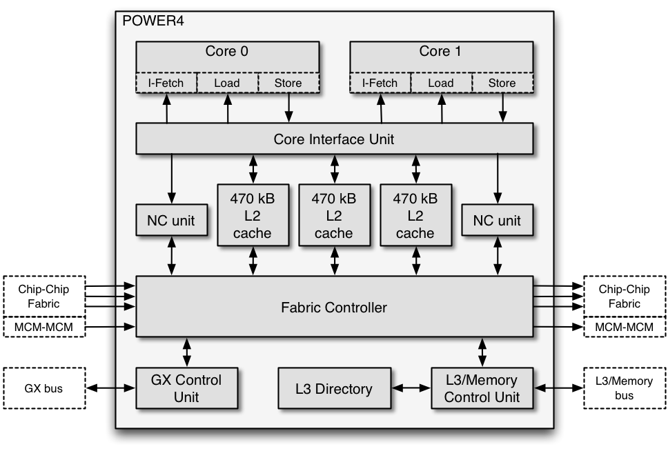
The POWER4 has a unified L2 cache, divided into three equal parts. Each has its own independent L2 controller which can feed 32 bytes of data per cycle. The Core Interface Unit (CIU) connects each L2 controller to either the data cache or instruction cache in either of the two processors. The Non-Cacheable (NC) Unit is responsible for handling instruction serializing functions and performing any noncacheable operations in the storage topology. There is an L3 cache controller, but the actual memory is off-chip. The GX bus controller controls I/O device communications, and there are two 4-byte wide GX buses, one incoming and the other outgoing. The Fabric Controller is the master controller for the network of buses, controlling communications for both L1/L2 controllers, communications between POWER4 chips {4-way, 8-way, 16-way, 32-way} and POWER4 MCM's. Trace-and-Debug, used for First Failure Data Capture, is provided. There is also a Built In Self Test function (BIST) and Performance Monitoring Unit (PMU). Power-on reset (POR) is supported.
Execution units
The POWER4 implements a superscalar microarchitecture through high-frequency speculative out-of-order execution using eight independent execution units. They are: two floating-point units (FP1-2), two load-store units (LD1-2), two fixed-point units (FX1-2), a branch unit (BR), and a conditional-register unit (CR). These execution units can complete up to eight operations per clock (not including the BR and CR units):
- each floating point unit can complete one fused multiply–add per clock (two operations),
- each load–store unit can complete one instruction per clock,
- each fixed-point unit can complete one instruction per clock.
The pipeline stages are:
- Branch Prediction
- Instruction Fetch
- Decode, Crack and Group Formation
- Group Dispatch and Instruction Issue
- Load–Store Unit Operation
- Load Hit Store
- Store Hit Load
- Load Hit Load
- Instruction Execution Pipeline
Multi-chip configuration
The POWER4 also came in a configuration using a multi-chip module (MCM) containing four POWER4 dies in a single package, with up to 128 MB of shared L3 ECC cache per MCM.
Parametrics
| Clock GHz | 1.3 GHz | Power | Transistors | Gate L | Gate oxide | Metal-layer | pitch | thickness | M1 | M2 | M3-M5 | M6(MQ) | M7(LM) | Dielectric | Vdd | |||
|---|---|---|---|---|---|---|---|---|---|---|---|---|---|---|---|---|---|---|
| 115 W | 1.5 V @ 1.1 GHz | |||||||||||||||||
| 174 million | ||||||||||||||||||
| 90 nm | ||||||||||||||||||
| 2.3 nm | ||||||||||||||||||
| 500 nm | 310 nm | |||||||||||||||||
| 630 nm | 310 nm | |||||||||||||||||
| 630 nm | 20 nm | |||||||||||||||||
| 1260 nm | 920 nm | |||||||||||||||||
| 1260 nm | 920 nm | |||||||||||||||||
| ~4.2 | ||||||||||||||||||
| 1.6 V |
POWER4+

The POWER4+, released in 2003, was an improved version of the POWER4 that ran at up to 1.9 GHz. It contained 184 million transistors, measured 267 mm2, and was fabricated in a 0.13 μm SOI CMOS process with eight layers of copper interconnect.
Notes
References
- "Power4 Focuses on Memory Bandwidth". (6 October 1999). Microprocessor Report.
- "IBM's Power4 Unveiling Continues". (20 November 2000). Microprocessor Report.
References
- (2011-01-24). "IBM's Server Processors: The RS64 and the POWER". The CPU Shack Museum.
- William Stallings, ''Computer Organization and Architecture'', Seventh Edition, -pp 44
- (2006). "IBM POWER Roadmap". IBM.
This article was imported from Wikipedia and is available under the Creative Commons Attribution-ShareAlike 4.0 License. Content has been adapted to SurfDoc format. Original contributors can be found on the article history page.
Ask Mako anything about POWER4 — get instant answers, deeper analysis, and related topics.
Research with MakoFree with your Surf account
Create a free account to save articles, ask Mako questions, and organize your research.
Sign up freeThis content may have been generated or modified by AI. CloudSurf Software LLC is not responsible for the accuracy, completeness, or reliability of AI-generated content. Always verify important information from primary sources.
Report