From Surf Wiki (app.surf) — the open knowledge base
Plasmonic nanolithography
Plasmonic nanolithography (also known as plasmonic lithography or plasmonic photolithography) is a nanolithographic process that utilizes surface plasmon excitations such as surface plasmon polaritons (SPPs) to fabricate nanoscale structures. SPPs, which are surface waves that propagate in between planar dielectric-metal layers in the optical regime, can bypass the diffraction limit on the optical resolution that acts as a bottleneck for conventional photolithography.
Theory
Main article: Surface plasmon polariton
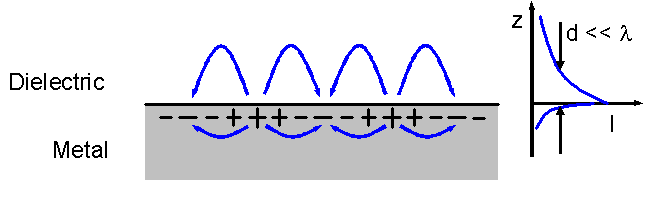
Surface plasmon polaritons are surface electromagnetic waves that propagate in between two surfaces with sign-changing permittivities. They originate from coupling of photons to plasma oscillations, quantized as plasmons. SPPs result in evanescent fields that decay perpendicularly to the interface where the propagation occurs. The dispersion relation for SPPs permits the excitation of wavelengths shorter than the free-space wavelength of the inbound light, additionally ensuring subwavelength field confinement. Nevertheless, the excitation of SPPs necessitate momentum mismatch; prism and grating coupling methods are common. For plasmonic nanolithography processes, this is achieved through surface roughness and perforations.
Methods

Plasmonic contact lithography, a modification on the evanescent near-field lithography, uses a metal photomask, on which the SPPs are excited. Similar to common photolithographic processes, photoresist is exposed to SPPs that propagate from the mask. Photomasks with holes enable grating coupling of SPPs; the fields only propagate for nanometers. Srituravanich et al. has demonstrated the lithographic process experimentally with a 2D silver hole array mask; 90 nm hole arrays were produced at 365 nm wavelength, which is beyond diffraction limit. Zayats and Smolyaninov utilized a multi-layered metal film mask to enhance the subwavelength aperture; such structures can be realized by thin film deposition methods. Bowtie apertures and nanogaps were also suggested as alternative apertures. A version of the method, named as surface plasmon interference nanolithography by Liu et al., uses SPP interference patterns. Despite offering high resolution and throughput, plasmonic contact lithography is regarded as an expensive and complex method; contamination due to contact is also a limiting factor.
Planar lens imaging nanolithography uses plasmonic lenses or negative-index superlenses, which were first proposed by John Pendry. Many superlens designs, such as Pendry's thin silver film or Fang et al.'s superlens, benefit from plasmonic excitations to focus Fourier components of incoming light beyond the diffraction limit. Chaturvedi et al. has demonstrated the imaging of a 30 nm chromium grating through silver superlens photolithography at 380 nm, while Shi et al. simulated a 20 nm lithography resolution at 193 nm wavelength with an aluminum superlens. Srituravanich et al. has developed a mechanically adjustable, hovering plasmonic lens for maskless near-field nanolithography, whereas another maskless approach by Pan et al. uses a "multi-stage plasmonic lens" for progressive coupling.
Plasmonic direct writing is a maskless form of photolithography that is based on scanning probe lithography; the method uses localized surface plasmon (LSP) enhancements from embedded plasmonic scanning probes to expose the photoresist. Wang et al. experimentally demonstrated 100 nm field confinement with this method. Kim et al. has developed a ~50 nm resolution scanning probe with a patterning speed of ~10 mm/s. Gold nanoparticles and other plasmonic nanostructures such as nanogaps have been used as masks for lithography; etching in this case can be achieved through either through photomasking principles or enhanced local heating in the vicinity of the nanostructure due to the LSP resonances. Lin et al. also used localized thermal excitations in gold nanoparticles to fabricate two-dimensional structures such as patterned graphene and molybdenum disulfide monolayers in a process termed as "optothermoplasmonic nanolithography." Photochemical effects of LSP resonances were also used as a catalyst in lithographic processes: Saito et al. demonstrated selective etching of silver nanocubes on titanium dioxide substrates by the means of plasmon-induced charge separation.
References
References
- (2016). "Towards do-it-yourself planar optical components using plasmon-assisted etching". [[Nature Communications]].
- (2013). "Nanolithography by Plasmonic Heating and Optical Manipulation of Gold Nanoparticles". [[ACS Nano]].
- (12 October 2008). "Flying plasmonic lens in the near field for high-speed nanolithography". [[Nature Nanotechnology]].
- (2009). "Plasmonic nano lithography with a high scan speed contact probe". [[Optics Express]].
- (2005). "Surface plasmon interference nanolithography". [[Nano Letters]].
- (2018). "Optothermoplasmonic Nanolithography for On-Demand Patterning of 2D Materials". [[Advanced Functional Materials]].
- (2009). "193nm superlens imaging structure for 20nm lithography node". [[Optics Express]].
- (29 November 2011). "Maskless plasmonic lithography at 22 nm resolution". [[Scientific Reports]].
- (2014). "Modern Plasmonics". [[Elsevier]].
- (6 December 2007). "Surface plasmon-based nanopatterning assisted by gold nanospheres". [[Nanotechnology (journal).
- (31 May 2011). "Plasmonic nanolithography: a review". Plasmonics.
- (2016). "Site-Selective Plasmonic Etching of Silver Nanocubes". [[The Journal of Physical Chemistry Letters]].
- (2008). "Plasmonic nearfield scanning probe with high transmission". [[Nano Letters]].
- (2005). "Surface-plasmon-assisted nanoscale photolithography by polarized light". [[Applied Physics Letters]].
- (25 January 2010). "A smooth optical superlens". [[Applied Physics Letters]].
- (2004). "Plasmonic nanolithography". [[Nano Letters]].
- (2017). "Light-directed growth of metal and semiconductor nanostructures". [[Journal of Materials Chemistry C]].
- (2010). "Nanogap-Assisted Surface Plasmon Nanolithography". [[The Journal of Physical Chemistry Letters]].
- (2019). "Plasmon-assisted nanojet lithography". [[Nanoscale (journal).
This article was imported from Wikipedia and is available under the Creative Commons Attribution-ShareAlike 4.0 License. Content has been adapted to SurfDoc format. Original contributors can be found on the article history page.
Ask Mako anything about Plasmonic nanolithography — get instant answers, deeper analysis, and related topics.
Research with MakoFree with your Surf account
Create a free account to save articles, ask Mako questions, and organize your research.
Sign up freeThis content may have been generated or modified by AI. CloudSurf Software LLC is not responsible for the accuracy, completeness, or reliability of AI-generated content. Always verify important information from primary sources.
Report