From Surf Wiki (app.surf) — the open knowledge base
Integrated circuit layout
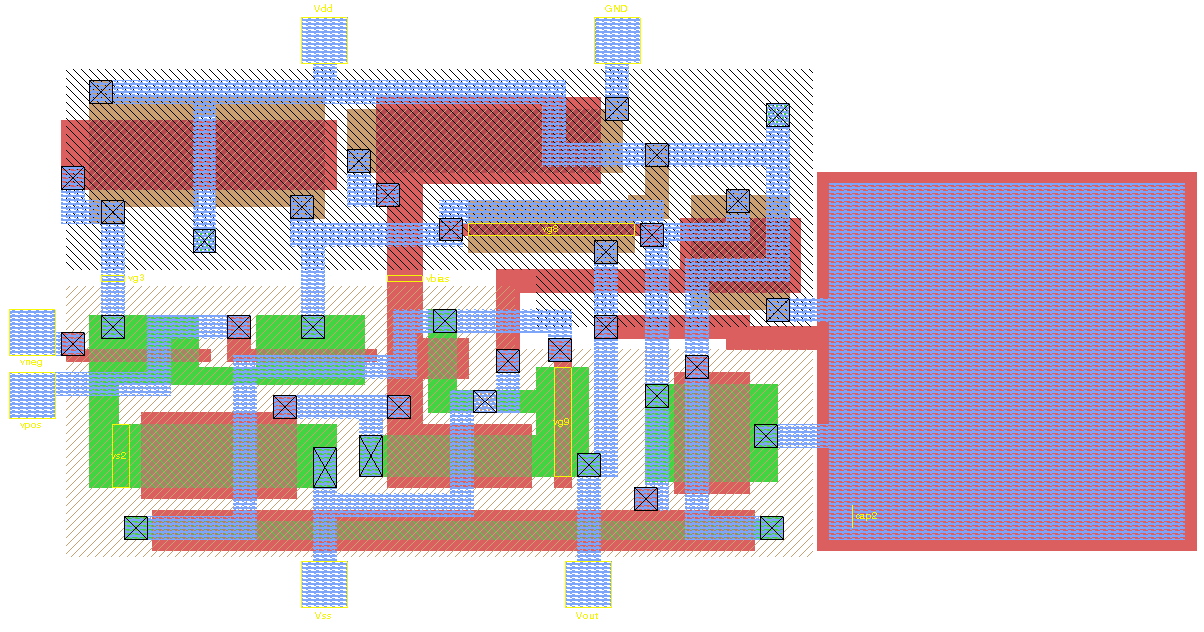
Representation of an integrated circuit's components as planar shapes
Representation of an integrated circuit's components as planar shapes
In integrated circuit design, integrated circuit (IC) layout, also known IC mask layout or mask design, is the representation of an integrated circuit in terms of planar geometric shapes which correspond to the patterns of metal, oxide, or semiconductor layers that make up the components of the integrated circuit. Originally the overall process was called tapeout, as historically early ICs used graphical black crepe tape on mylar media for photo imaging (erroneously believed to reference magnetic data—the photo process greatly predated magnetic media).
When using a standard process—where the interaction of the many chemical, thermal, and photographic variables is known and carefully controlled—the behaviour of the final integrated circuit depends largely on the positions and interconnections of the geometric shapes. Using a computer-aided layout tool, the layout engineer—or layout technician—places and connects all of the components that make up the chip such that they meet certain criteria—typically: performance, size, density, and manufacturability. This practice is often subdivided between two primary layout disciplines: analog and digital.
The generated layout must pass a series of checks in a process known as physical verification. The most common checks in this verification process are
- Design rule checking (DRC),
- Layout versus schematic (LVS),
- parasitic extraction,
- antenna rule checking, and
- electrical rule checking (ERC).
When all verification is complete, layout post processing is applied where the data is also translated into an industry-standard format, typically GDSII, and sent to a semiconductor foundry. The milestone completion of the layout process of sending this data to the foundry is now colloquially called "tapeout". The foundry converts the data into mask data and uses it to generate the photomasks used in a photolithographic process of semiconductor device fabrication.
In the earlier, simpler, days of IC design, layout was done by hand using opaque tapes and films, an evolution derived from early days of printed circuit board (PCB) design -- tape-out.
Modern IC layout is done with the aid of IC layout editor software, mostly automatically using EDA tools, including place and route tools or schematic-driven layout tools. Typically this involves a library of standard cells.
The manual operation of choosing and positioning the geometric shapes is informally known as "polygon pushing". Dirk Jansen, editor. "The Electronic Design Automation Handbook". 2010. p. 39. Dan Clein. "CMOS IC Layout: Concepts, Methodologies, and Tools". 1999 p. 60. "Conference Record". 1987. p. 118. Charles A. Harper; Harold C. Jones. "Active Electronic Component Handbook". 1996. p. 2 Riko Radojcic. "Managing More-than-Moore Integration Technology Development". 2018. p. 99
References
References
- A. Kahng, J. Lienig, I. Markov, J. Hu: ''VLSI Physical Design: From Graph Partitioning to Timing Closure'', {{doi. 10.1007/978-3-030-96415-3, {{ISBN. 978-3-030-96414-6, p. 9.
- Basu, Joydeep. (2019-10-09). "From Design to Tape-out in SCL 180 nm CMOS Integrated Circuit Fabrication Technology". IETE Journal of Education.
- J. Lienig, J. Scheible. (2020). "Fundamentals of Layout Design for Electronic Circuits". Springer.
This article was imported from Wikipedia and is available under the Creative Commons Attribution-ShareAlike 4.0 License. Content has been adapted to SurfDoc format. Original contributors can be found on the article history page.
Ask Mako anything about Integrated circuit layout — get instant answers, deeper analysis, and related topics.
Research with MakoFree with your Surf account
Create a free account to save articles, ask Mako questions, and organize your research.
Sign up freeThis content may have been generated or modified by AI. CloudSurf Software LLC is not responsible for the accuracy, completeness, or reliability of AI-generated content. Always verify important information from primary sources.
Report