From Surf Wiki (app.surf) — the open knowledge base
Conductive atomic force microscopy
Method of measuring the microscopic topography of a material
_and_current_(right)_maps_collected_with_CAFM_on_a_polycrystalline_HfO2_stack.png)
Method of measuring the microscopic topography of a material
In microscopy, conductive atomic force microscopy (C-AFM) or current sensing atomic force microscopy (CS-AFM) is a mode in atomic force microscopy (AFM) that simultaneously measures the topography of a material and the electric current flow at the contact point of the tip with the surface of the sample. The topography is measured by detecting the deflection of the cantilever using an optical system (laser + photodiode), while the current is detected using a current-to-voltage preamplifier. The fact that the CAFM uses two different detection systems (optical for the topography and preamplifier for the current) is a strong advantage compared to scanning tunneling microscopy (STM). Basically, in STM the topography picture is constructed based on the current flowing between the tip and the sample (the distance can be calculated depending on the current). Therefore, when a portion of a sample is scanned with an STM, it is not possible to discern if the current fluctuations are related to a change in the topography (due to surface roughness) or to a change in the sample conductivity (due to intrinsic inhomogeneities).
The CAFM is usually operated in contact mode; the tip can be kept at one location while the voltage and current signals are applied/read, or it can be moved to scan a specific region of the sample under a constant voltage (and the current is collected). Recently, some manufacturers provide the option of measuring the current in semi-contact mode. The CAFM was first developed by Sean O'Shea and co-workers at the University of Cambridge in 1993, and it is referred to in the literature by several names, including C-AFM, local-conductivity AFM (LC-AFM), conductive probe AFM (CP-AFM), conductive scanning probe microscopy (C-SPM) or conductive scanning force microscopy (C-SFM), although CAFM is the most widespread.
Working principle
In order to transform an AFM into a CAFM, three elements are required: i) the probe tip must be conductive, ii) a voltage source is needed to apply a potential difference between the tip and the sample holder, and iii) a preamplifier is used to convert the (analogical) current signal into (digital) voltages that can be read by the computer. In CAFM experiments, the sample is usually fixed on the sample holder using a conductive tape or paste, being silver paints the most widespread. A Faraday cage is also convenient to isolate the sample from any external electrical interference. Using this setup, when a potential difference is imposed between tip and sample an electrical field is generated, which results in a net current flowing from tip-to-sample or vice versa. The currents collected by the CAFM obey the relationship:
I = J \cdot A_{eff}
where I is the total current flowing through the tip/sample nanojunction, J is the current density and Aeff is the effective emission area through which electrons can flow (from now on we will refer to it just as effective area). The most common mistake in CAFM research is to assume that the effective emission area (Aeff) equals the physical contact area (Ac). Strictly, this assumption is erroneous because in many different tip/sample systems the electrical field applied may propagate laterally. For example, when the CAFM tip is placed on a metal the lateral conductivity of the sample is very high, making (in principle) the whole sample surface area electrically connected (Aeff equals the area covered by the metallic film/electrode). Aeff has been defined as:"the sum of all those infinitesimal spatial locations on the surface of the sample that are electrically connected to the CAFM tip (the potential difference is negligible). As such, Aeff is a virtual entity that summarizes all electrically relevant effects within the tip/sample contact system into a single value, over which the current density is assumed to be constant." Therefore, when the CAFM tip is placed in contact with a metal (a metallic sample or just a metallic pad on an insulator), the lateral conductivity of the metal is very high, and the CAFM tip can be understood as a current collector (nanosized probe station); on the contrary, if the CAFM tip is placed directly on an insulator, it acts as a nanosized electrode and provides a very high lateral resolution. The value of Aeff when a Pt-Ir coated tip (with a typical radius of 20 nm) is placed on a SiO2 insulating film has been calculated to be typically 50 nm2. The value of Aeff can fluctuate depending on the environmental conditions, and it can range from 1 nm2 in ultra high vacuum (UHV) to 300 nm2 in very humid environments. On well-defined single crystal surfaces under UHV conditions it has even been demonstrated that measurements of the local conductivity with atomic resolution are possible.
Issues with conventional CAFM
Common problems in conventional CAFM include difficulty in managing high and low currents and avoiding unwanted side-effects such as the Joule, Bimetallic and local oxidation effects when using high currents. In order to produce accurate and reproducible measurements, frequent tip replacements and repeated experimental setup can be required. A book edited by Mario Lanza discusses these issues (Chapter 12, Pacheco and Martinez. 2017). This chapter, written by employees of AFM manufacturer Concept Scientific Instruments, claims that their company's module named ResiScope overcomes these issues, and provide supporting data, without any supporting peer-reviewed publication.
In order to overcome the narrow dynamic range limitations of conventional preamplifiers, advanced modules such as the ResiScope have been developed. The ResiScope allows for resistance measurements across a wide dynamic range — spanning over ten decades — from approximately 10² Ω to 10¹² Ω, while maintaining high spatial resolution. This capability enables the detailed study of materials with both low and high conductivity on the nanoscale.
Applications


Apart from monitoring the electrical properties of a dielectric, the CAFM can be also used to alter its properties by applying an electrical field locally. In particular, the CAFM is especially useful to determine which locations of the samples lead to premature BD, which can provide essential information about the reliability of the samples. The CAFM also helped to confirm the percolation theory of the BD by experimentally proving that this is a very local phenomenon that occurs in small areas typically below 100 nm2. Lateral propagations of the BD event can also be detected by CAFM. The severity of the BD event can also be studied from the dielectric breakdown induced epitaxy, which can be observed from subsequent topographic images collected with the CAFM after the voltage ramp. Similarly, the analysis of the BD recovery (resistive switching, RS) can also be monitored by CAFM. All the capabilities of the CAFM for studying resistive switching in dielectrics have been summarized in the review article of reference. Unlike a normal AFM, the CAFM can be also used to perform local photolithography via bias-assisted local anodic oxidation (LAO). Nowadays the CAFM technique has expanded to many other fields of science, including physics, materials science, chemistry and engineering (among many others), and it has been used to study different materials and/or structures, including nanoparticles, molecules, nanowires, carbon nanotubes, two dimensional (2D) materials, coatings, photoelectricity and piezoelectricity (among others). As of June 14 of 2016, the CAFM had been used in 1325 journal research articles, and it has become a popular tool in nanosciences.
Challenges of CAFM on soft materials
There is now an increasing use of the electrical characterisation capabilities of AFM in nanotechnology-based fields such as energy harvesting, organic/polymer-based electronics, semiconductors etc. Flexible electronics based on organic compounds are gaining popularity as soft electrical materials.
Currently, two different methods are used for Conductive AFM (C-AFM) measurements of soft materials such as conductive polymers.
Sinusoidal Regime Method
In the Sinusoidal Regime method, the cantilever is mechanically excited in the range of 100–2000 Hz i.e. well below its natural resonance frequency. The tip of the cantilever interacts with the substrate periodically during the bottom part of its sinusoidal displacement. This method allows easy imaging of soft samples by controlling the amplitude of the movement of the tip. However, some quantitative measurements cannot be performed (electrical, thermal, etc…) because the force exerted by the tip on the sample is variable.
Linear Regime Method
The Linear Regime Method is based on the force versus distance spectroscopy curves. In this quasi-static approach, the cantilever follows an approach-retract cycle towards the sample with constant velocity. Hooke's law is used to select the force to be exerted. F=k*z, where F is the applied force, k is the cantilever constant and z is the cantilever deflection relative to the rest deflection position. However, this method is slow with an approach-retract cycle of 1 sec. At this rate, it can take up to 3 days to measure a standard 512 x 512 image.
A new approach to resolve these issues is the Soft ResiScope mode which combines fast point contacts and constant force.
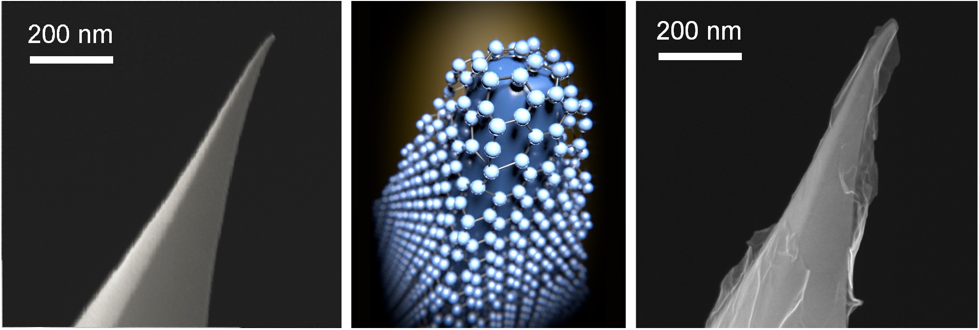
CAFM probes
The preamplifier

References
References
- Lanza, Mario. (2017). "Conductive Atomic Force Microscopy". Wiley-VCH.
- "PeakForce TUNA - Bruker AFM Probes".
- (1993-02-15). "Spatially resolved electrical measurements of SiO2 gate oxides using atomic force microscopy". Applied Physics Letters.
- "Silver Paints/Pastes : SPI Supplies".
- (2012-11-29). "Influence of parasitic capacitances on conductive AFM I-V measurements and approaches for its reduction". Journal of Vacuum Science & Technology B, Nanotechnology and Microelectronics: Materials, Processing, Measurement, and Phenomena.
- (July 2009). "Comparative study between conventional macroscopic IV techniques and advanced AFM based methods for electrical characterization of dielectrics at the nanoscale". Microelectronic Engineering.
- (2007-01-30). "C-AFM-based thickness determination of thin and ultra-thin SiO2 films by use of different conductive-coated probe tips". Applied Surface Science.
- (2014-05-04). "Analysis of Factors in the Nanoscale Physical and Electrical Characterization of High-K Materials by Conductive Atomic Force Microscope". Integrated Ferroelectrics.
- (2013-10-01). "Leakage current through the poly-crystalline HfO2: Trap densities at grains and grain boundaries". Journal of Applied Physics.
- (2009-12-01). "Combined Nanoscale and Device-Level Degradation Analysis of Layers of MOS Nonvolatile Memory Devices". IEEE Transactions on Device and Materials Reliability.
- (September 2009). "Trapped charge and stress induced leakage current (SILC) in tunnel SiO2 layers of de-processed MOS non-volatile memory devices observed at the nanoscale". Microelectronics Reliability.
- (July 2009). "Crystallization and silicon diffusion nanoscale effects on the electrical properties of Al2O3 based devices". Microelectronic Engineering.
- (September 2007). "Influence of the manufacturing process on the electrical properties of thin (<4 nm) Hafnium based high-k stacks observed with CAFM". Microelectronics Reliability.
- (2010-10-01). "Note: Electrical resolution during conductive atomic force microscopy measurements under different environmental conditions and contact forces". Review of Scientific Instruments.
- (September 2010). "UHV CAFM characterization of high-k dielectrics: Effect of the technique resolution on the pre- and post-breakdown electrical measurements". Microelectronics Reliability.
- (2011-01-31). "Polycrystallization effects on the nanoscale electrical properties of high-k dielectrics". Nanoscale Research Letters.
- (2018). "Local surface conductivity of transition metal oxides mapped with true atomic resolution". Nanoscale.
- (15 June 2024). "The most advanced module for Conductive AFM".
- F. Levesque, C. Durand, A. Barthel, and A. De Martino. "The ResiScope: New Technique for Mapping Resistance at the Nanoscale." ''Microscopy Today'', vol. 23, no. 6, 2015, pp. 32–37. [https://academic.oup.com/mt/article-abstract/23/6/32/6815337]
- (1995-09-01). "Conducting atomic force microscopy study of silicon dioxide breakdown". Journal of Vacuum Science & Technology B: Microelectronics and Nanometer Structures Processing, Measurement, and Phenomena.
- (1996-01-01). "High resolution Fowler-Nordheim field emission maps of thin silicon oxide layers". Applied Physics Letters.
- (1998-03-01). "1998 IEEE International Reliability Physics Symposium Proceedings 36th Annual (Cat No 98CH36173) RELPHY-98".
- (1998-11-19). "Conducting atomic force microscopy for nanoscale electrical characterization of thin SiO2". Applied Physics Letters.
- (June 1999). "A new AFM-based tool for testing dielectric quality and reliability on a nanometer scale". Microelectronics Reliability.
- (1996-04-01). "Proceedings of International Reliability Physics Symposium RELPHY-96".
- (2006). "Thickness determination of thin and ultra-thin SiO2 films by C-AFM IV-spectroscopy". Applied Surface Science.
- (March 2007). "Evaluation of trap creation and charging in thin SiO2 using both SCM and C-AFM". Microelectronic Engineering.
- (2009-12-24). "Trap-assisted tunneling hole injection in SiO2: Experiment and theory". Journal of Experimental and Theoretical Physics.
- (2006-05-29). "Conductive atomic force microscopy studies of thin SiO2 layer degradation". Applied Physics Letters.
- (2006-03-01). "Two-trap-assisted tunneling model for post-breakdown I-V characteristics in ultrathin silicon dioxide". IEEE Transactions on Device and Materials Reliability.
- (2004-04-13). "Nanoscale electrical characterization of trap-assisted quasibreakdown fluctuations in SiO2". Applied Physics Letters.
- (2001-12-01). "International Electron Devices Meeting. Technical Digest (Cat. No.01CH37224)".
- (2002-01-29). "Electrical characterization of stressed and broken down SiO2 films at a nanometer scale using a conductive atomic force microscope". Journal of Applied Physics.
- (2010-07-25). "Low voltage stress-induced leakage current in HfO2 dielectric films". Materials Science and Engineering: B.
- (2008-05-12). "Polarity dependent breakdown of the high-κ/SiOx gate stack: A phenomenological explanation by scanning tunneling microscopy". Applied Physics Letters.
- (2004-10-01). "Proceedings. 7th International Conference on Solid-State and Integrated Circuits Technology, 2004".
- (2011-03-01). "Conductivity and Charge Trapping After Electrical Stress in Amorphous and Polycrystalline Devices Studied With AFM-Related Techniques". IEEE Transactions on Nanotechnology.
- (2011-09-01). "Nanoscale and Device Level Gate Conduction Variability of High-k Dielectrics-Based Metal-Oxide-Semiconductor Structures". IEEE Transactions on Device and Materials Reliability.
- (June 2013). "Nanoscale and device level electrical behavior of annealed ALD Hf-based gate oxide stacks grown with different precursors". Microelectronics Reliability.
- (2010-12-15). "Correlation between growth kinetics and nanoscale resistive switching properties of SrTiO3 thin films". Journal of Applied Physics.
- (2007-06-01). "Nanoscale Bias-Annealing Effect in Postirradiated Thin Silicon Dioxide Films Observed by Conductive Atomic Force Microscopy". IEEE Transactions on Device and Materials Reliability.
- (February 2007). "Reliability study of ultrathin oxide films subject to irradiation-then-stress treatment using conductive atomic force microscopy". Microelectronics Reliability.
- (2009-01-01). "Implanted and irradiated SiO2/Si structure electrical properties at the nanoscale". Journal of Vacuum Science & Technology B: Microelectronics and Nanometer Structures Processing, Measurement, and Phenomena.
- (2005). "Comparison of SiO2 and HfO2/SiO2 gate stacks electrical behaviour at a nanometre scale with CAFM". Electronics Letters.
- (February 2008). "Breakdown spots propagation in ultra-thin SiO2 films under repetitive ramped voltage stress using conductive atomic force microscopy". Journal of Physics and Chemistry of Solids.
- (2002-09-01). "Polarity-dependent dielectric breakdown-induced epitaxy (DBIE) in Si MOSFETs". IEEE Electron Device Letters.
- (2009-07-15). "Physical degradation of gate dielectrics induced by local electrical stress using conductive atomic force microscopy". Journal of Applied Physics.
- (2003-06-10). "Atomic force microscope topographical artifacts after the dielectric breakdown of ultrathin SiO2 films". Surface Science.
- (2012-11-05). "Resistive switching in hafnium dioxide layers: Local phenomenon at grain boundaries". Applied Physics Letters.
- (2012-03-19). "Grain boundaries as preferential sites for resistive switching in the HfO2 resistive random access memory structures". Applied Physics Letters.
- (2015-04-01). "In Situ Demonstration of the Link Between Mechanical Strength and Resistive Switching in Resistive Random-Access Memories". Advanced Electronic Materials.
- (2014-08-08). "(Invited) Elucidating the Origin of Resistive Switching in Ultrathin Hafnium Oxides through High Spatial Resolution Tools". ECS Transactions.
- Lanza, Mario. (2014-03-13). "A Review on Resistive Switching in High-k Dielectrics: A Nanoscale Point of View Using Conductive Atomic Force Microscope". Materials.
- (2005-09-15). "Conducting Ni nanoparticles in an ion-modified polymer". Journal of Applied Physics.
- (2015-07-16). "Nanoscale characterization of PM2.5 airborne pollutants reveals high adhesiveness and aggregation capability of soot particles". Scientific Reports.
- (2001-10-19). "Reproducible Measurement of Single-Molecule Conductivity". Science.
- (2006-04-14). "Piezoelectric Nanogenerators Based on Zinc Oxide Nanowire Arrays". Science.
- (2000-03-14). "Electrical measurements of individual semiconducting single-walled carbon nanotubes of various diameters". Applied Physics Letters.
- (2010-12-27). "Correlation between the nanoscale electrical and morphological properties of crystallized hafnium oxide-based metal oxide semiconductor structures". Applied Physics Letters.
- (2011-03-29). "Nanoscale structural characterization of epitaxial graphene grown on off-axis 4H-SiC (0001)". Nanoscale Research Letters.
- (2011-01-31). "Lateral homogeneity of the electronic properties in pristine and ion-irradiated graphene probed by scanning capacitance spectroscopy". Nanoscale Research Letters.
- (2016-01-04). "Boron nitride as two dimensional dielectric: Reliability and dielectric breakdown". Applied Physics Letters.
- (2013-05-21). "Electrical and mechanical performance of graphene sheets exposed to oxidative environments". Nano Research.
- (2004-09-01). "Resonance Tunneling Diode Structures on CdTe Nanowires Made by Conductive AFM". Nano Letters.
- (2017-01-26). "High-resolution characterization of hexagonal boron nitride coatings exposed to aqueous and air oxidative environments". Nano Research.
- (2014-09-04). "Ageing mechanisms and reliability of graphene-based electrodes". Nano Research.
- (2013-11-13). "Spatial Mapping of Efficiency of GaN/InGaN Nanowire Array Solar Cells Using Scanning Photocurrent Microscopy". Nano Letters.
- (2016-04-21). "Suppression of nanowire clustering in hybrid energy harvesters". J. Mater. Chem. C.
- (17 June 2024). "The best Conductive AFM for polymers and soft materials".
- "NanoWorld".
- "National Instriuments".
- (1990-07-15). "Performance limits for the scanning tunneling microscope". Journal of Applied Physics.
- "FEMTO".
- (2013-03-13). "Graphene-Coated Atomic Force Microscope Tips for Reliable Nanoscale Electrical Characterization". Advanced Materials.
- (2016-04-21). "Moving graphene devices from lab to market: advanced graphene-coated nanoprobes". Nanoscale.
- (2008-07-01). "Improving the electrical performance of a conductive atomic force microscope with a logarithmic current-to-voltage converter". Review of Scientific Instruments.
This article was imported from Wikipedia and is available under the Creative Commons Attribution-ShareAlike 4.0 License. Content has been adapted to SurfDoc format. Original contributors can be found on the article history page.
Ask Mako anything about Conductive atomic force microscopy — get instant answers, deeper analysis, and related topics.
Research with MakoFree with your Surf account
Create a free account to save articles, ask Mako questions, and organize your research.
Sign up freeThis content may have been generated or modified by AI. CloudSurf Software LLC is not responsible for the accuracy, completeness, or reliability of AI-generated content. Always verify important information from primary sources.
Report