From Surf Wiki (app.surf) — the open knowledge base
Cadmium arsenide
| NFPA-F = 1 | NFPA-H = 4 | NFPA-R = 0 | NFPA-S = W
Cadmium arsenide (Cd3As2) is an inorganic semimetal in the II-V family. It exhibits the Nernst effect.
Properties
Thermal
Cd3As2 dissociates between 220 and 280 °C according to the reaction
:2 Cd3As2(s) → 6 Cd(g) + As4(g)
An energy barrier was found for the nonstoichiometric vaporization of arsenic due to the irregularity of the partial pressures with temperature. The range of the energy gap is from 0.5 to 0.6 eV. Cd3As2 melts at 716 °C and changes phase at 615 °C/
Phase transition
Pure cadmium arsenide undergoes several phase transitions at high temperatures, making phases labeled α (stable), α', α" (metastable), and β. At 593° the polymorphic transition α → β occurs.
:α-Cd3As2 ↔ α'-Cd3As2 occurs at ~500 K. :α'-Cd3As2 ↔ α'-Cd3As2 occurs at ~742 K and is a regular first order phase transition with marked hysteresis loop. :α"-Cd3As2 ↔ β-Cd3As2 occurs at 868 K.
Single crystal x-ray diffraction was used to determine the lattice parameters of Cd3As2 between 23 and 700 °C. Transition α → α′ occurs slowly and therefore is most likely an intermediate phase. Transition α′ → α″ occurs much faster than α → α′ and has very small thermal hysteresis. This transition results in a change in the fourfold axis of the tetragonal cell, causing crystal twinning. The width of the loop is independent of the rate of heating although it becomes narrower after several temperature cycles.
Electronic
The compound cadmium arsenide has a lower vapor pressure (0.8 atm) than both cadmium and arsenic separately. Cadmium arsenide does not decompose when it is vaporized and re-condensed. Carrier Concentration in Cd3As2 are usually (1–4)×1018 electrons/cm3. Despite having high carrier concentrations, the electron mobilities are also very high (up to 10,000 cm2/(V·s) at room temperature).
In 2014 Cd3As2 was shown to be a semimetal material analogous to graphene that exists in a 3D form that should be much easier to shape into electronic devices.
Conducting
Cadmium arsenide is a II-V semiconductor showing degenerate n-type semiconductor intrinsic conductivity with a large mobility, low effective mass and highly non parabolic conduction band, or a Narrow-gap semiconductor. It displays an inverted band structure, and the optical energy gap, eg, is less than 0. When deposited by thermal evaporation (deposition), cadmium arsenide displayed the Schottky (thermionic emission) and Poole–Frenkel effect at high electric fields.
Magnetoresistance
Cadmium Arsenide shows very strong quantum oscillations in resistance even at the relatively high temperature of 100K. This makes it useful for testing cryomagnetic systems as the presence of such a strong signal is a clear indicator of function.
Preparation
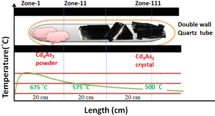
Cadmium arsenide can be prepared as amorphous semiconductive glass. According to Hiscocks and Elliot, the preparation of cadmium arsenide was made from cadmium metal, which had a purity of 6 N from Kock-Light Laboratories Limited. Hoboken supplied β-arsenic with a purity of 99.999%. Stoichiometric proportions of the elements cadmium and arsenic were heated together. Separation was difficult and lengthy due to the ingots sticking to the silica and breaking. Liquid encapsulated Stockbarger growth was created. Crystals are pulled from volatile melts in liquid encapsulation. The melt is covered by a layer of inert liquid, usually B2O3, and an inert gas pressure greater than the equilibrium vapor pressure is applied. This eliminates the evaporation from the melt which allows seeding and pulling to occur through the B2O3 layer.
Crystal structure
The unit cell of Cd3As2 is tetragonal with either primitive or body-centered centering depending on the polymorph. The arsenic ions are cubic close packed and the cadmium ions are tetrahedrally coordinated. The vacant tetrahedral sites provoked research by von Stackelberg and Paulus (1935), who determined the primary structure. Each arsenic ion is surrounded by cadmium ions at six of the eight corners of a distorted cube and the two vacant sites were at the diagonals.
The crystalline structure of cadmium arsenide is very similar to that of zinc phosphide (Zn3P2), zinc arsenide (Zn3As2) and cadmium phosphide (Cd3P2). These compounds of the Zn-Cd-P-As quaternary system exhibit full continuous solid solution.
Nernst effect
Cadmium arsenide is used in infrared detectors using the Nernst effect, and in thin-film dynamic pressure sensors. It can be also used to make magnetoresistors, and in photodetectors.
Cadmium arsenide can be used as a dopant for HgCdTe.
References
References
- (2015). "Large single crystal growth, transport property, and spectroscopic characterizations of three-dimensional Dirac semimetal Cd3As2". Scientific Reports.
- (2014). "The Crystal and Electronic Structures of Cd3As2, the Three-Dimensional Electronic Analogue of Graphene". Inorganic Chemistry.
- {{PGCH. 0087
- (1964). "Mass Spectrometric Study of the Nonstoichiometric Vaporization of Cadmium Arsenide1". The Journal of Physical Chemistry.
- (1969). "On the preparation, growth and properties of Cd3As2". Journal of Materials Science.
- (1969). "A refinement of the crystal structure of α"-Cd3As2". Acta Crystallographica Section B.
- (1973). "Thermal expansion and phase transitions of Cd3As2 and Zn3As2". Physica Status Solidi A.
- (1979). "Inverted band structure of Cd3As2". Physica Status Solidi B.
- (2014). "Observation of a three-dimensional topological Dirac semimetal phase in high-mobility Cd3As2". Nature Communications.
- (2014). "A stable three-dimensional topological Dirac semimetal Cd3As2". Nature Materials.
- (2006). "Van der Pauw resistivity measurements on evaporated thin films of cadmium arsenide, Cd3As2". Applied Surface Science.
- (19 March 2015). "Linear Magnetoresistance Caused by Mobility Fluctuations in -Doped". Physical Review Letters.
- (2019). "Point group symmetry of cadmium arsenide thin films determined by convergent beam electron diffraction". Physical Review Materials.
- (2014). "Compounds and solid solutions of the Zn-Cd-P-As system in semiconductor electronics". Inorganic Materials.
- (1998). "ICSE'98. 1998 IEEE International Conference on Semiconductor Electronics. Proceedings (Cat. No.98EX187)".
This article was imported from Wikipedia and is available under the Creative Commons Attribution-ShareAlike 4.0 License. Content has been adapted to SurfDoc format. Original contributors can be found on the article history page.
Ask Mako anything about Cadmium arsenide — get instant answers, deeper analysis, and related topics.
Research with MakoFree with your Surf account
Create a free account to save articles, ask Mako questions, and organize your research.
Sign up freeThis content may have been generated or modified by AI. CloudSurf Software LLC is not responsible for the accuracy, completeness, or reliability of AI-generated content. Always verify important information from primary sources.
Report