From Surf Wiki (app.surf) — the open knowledge base
Back-side bus
Computer architecture terminology

Computer architecture terminology
In personal computer microprocessor architecture, a back-side bus (BSB), or backside bus, was a computer bus used on early Intel platforms to connect the CPU to CPU cache memory, usually off-die L2. If a design utilizes a back-side bus along with a front-side bus (FSB), the design is said to use a dual-bus architecture, or in Intel's terminology Dual Independent Bus (DIB) architecture. The back-side bus architecture evolved when newer processors like the second-generation Pentium III began to incorporate on-die L2 cache, which at the time was advertised as Advanced Transfer Cache, but Intel continued to refer to the Dual Independent Bus till the end of Pentium III.
History
BSB is an improvement over the older practice of using a single system bus, because a single bus typically became a severe bottleneck as CPUs and memory speeds increased. Due to its dedicated nature, the back-side bus can be optimized for communication with cache, thus eliminating protocol overheads and additional signals that are required on a general-purpose bus. Furthermore, since a BSB operates over a shorter distance, it can typically operate at higher clock speeds, increasing the computer's overall performance.
Cache connected with a BSB was initially external to the microprocessor die, but now is usually on-die.{{cite web |url= http://www.itworld.com/Comp/1091/CWD010430STO60015/ |archiveurl= https://web.archive.org/web/20010502134148/http://www.itworld.com/Comp/1091/CWD010430STO60015/ |archivedate= 2001-05-02| title=Buses: frontside and backside| publisher=ITworld| date=2001-04-30}} In the latter case, the BSB clock frequency is typically equal to the processor's,{{cite web| url=http://www.itworld.com/Comp/1091/CWD010430STO60015/| archiveurl=https://web.archive.org/web/20010502134148/http://www.itworld.com/Comp/1091/CWD010430STO60015/| archivedate=2001-05-02| title=Buses: frontside and backside| publisher=ITworld| date=2001-04-30}} and the back-side bus can also be made much wider (256-bit, 512-bit) than either off-chip or on-chip FSB.
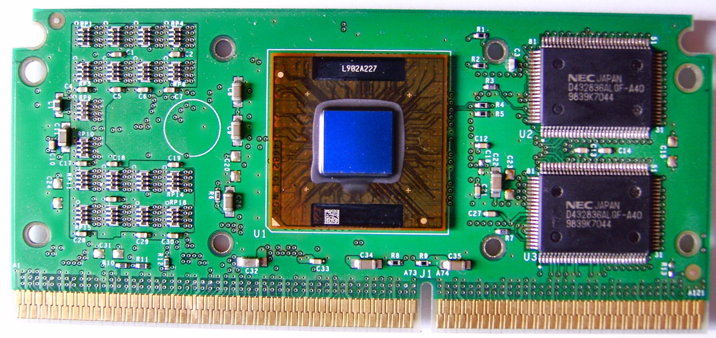
The dual-bus architecture was used in a number of designs, including the IBM and Freescale (formerly the semiconductor division of Motorola) PowerPC processors (certain PowerPC 604 models, the PowerPC 7xx family, and the Freescale 7xxx line), as well as the Intel Pentium Pro, Pentium II and early Pentium III processors,{{cite web| url=http://searchstorage.techtarget.com/sDefinition/0,,sid5_gci213804,00.html| title=Backside Bus| publisher=Whatis.com| date=2001-04-30}} which used it to access their L2 cache (earlier Intel processors accessed the L2 cache over the FSB, while later processors moved it on-chip).
References
References
- Kozierok, Charles M.. (2001-04-17). "Dedicated "Backside" Cache Bus".
- [http://download.intel.com/design/intarch/prodbref/27331106.pdf Pentium® III Processors for Applied Computing product brief]
- (1997-11-07). "Monday a big day for Apple". CNet.
This article was imported from Wikipedia and is available under the Creative Commons Attribution-ShareAlike 4.0 License. Content has been adapted to SurfDoc format. Original contributors can be found on the article history page.
Ask Mako anything about Back-side bus — get instant answers, deeper analysis, and related topics.
Research with MakoFree with your Surf account
Create a free account to save articles, ask Mako questions, and organize your research.
Sign up freeThis content may have been generated or modified by AI. CloudSurf Software LLC is not responsible for the accuracy, completeness, or reliability of AI-generated content. Always verify important information from primary sources.
Report